
682
MRS BULLETIN
•
VOLUME 37
•
JULY 2012
•
www.mrs.org/bulletin
© 2012 Materials Research Society
Introduction
Now, perhaps more than at any previous time, there is widespread
appreciation of the urgent need for new functional materials and
the critical role they play in matters of great importance to energy,
the environment, sustainability, and the economy. A number of
recent panel reports in the United States, including those coordi-
nated by the National Research Council (NRC),
1
the Department
of Energy,
2
and the Offi ce of Science and Technology Policy of
the National Science and Technology Council,
3
have emphasized
the importance of new, enabling materials in the economy and
the need to critically examine the current status and future pros-
pects. With support and encouragement from the US National
Science Foundation, the authors of this contribution organized
a workshop in 2011 on the theme of “Materials by Design”
( http :// www . mbd . mrl . ucsb . edu ). Broadly defi ned, “Materials by
Design” has the goal of achieving desired properties in materials
through appropriate tuning of composition, structure, and architec-
ture, which enables a given application. The expertise represented
at the workshop ranged from solid-state chemistry, to organic,
hybrid, nano, and liquid crystalline materials, to crystal growth,
condensed matter experiment, and included both pencil-and-paper
and computational theory. The questions of most interest to the
participants were: How does one go about increasing the effi cien-
cies in the process of new materials development, and concurrently
to achieve this end, how does one make better, more effective use
of theory and computation?
While the workshop participants were primarily based in the
United States, we believe the fi ndings presented have global rel-
evance. Indeed, the integrated approaches to “Materials by Design”
lend themselves very well to international collaborations.
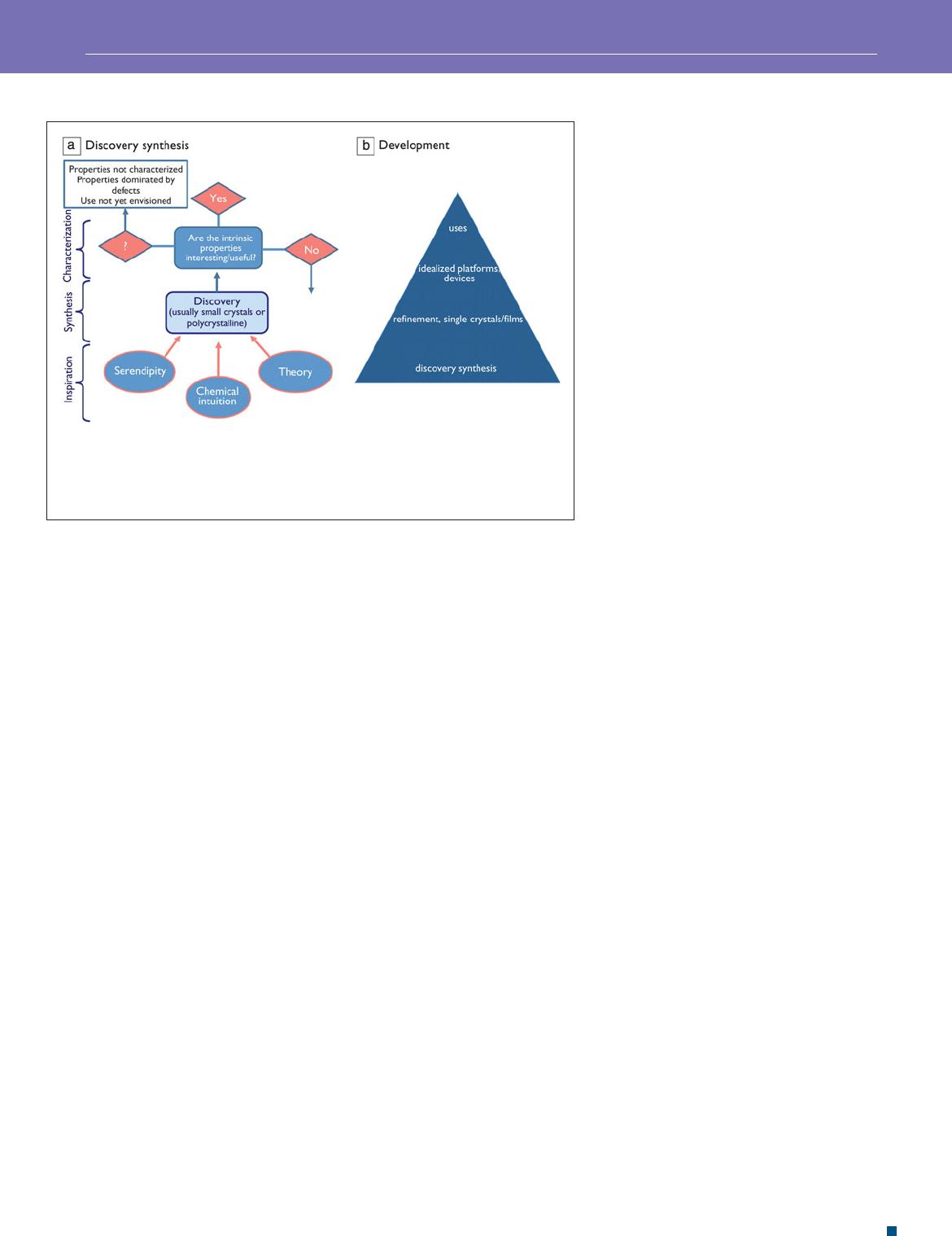
As a starting point, we consider a typical fl owchart
( Figure 1 a) depiction of the process of envisioning/designing
and preparing a new material for a particular application, also
sometimes referred to as discovery synthesis. Theory and chem-
ical intuition—often in conjunction with the known literature—
can combine to suggest a target material, but in many cases,
the material produced is not that intended, so the role of
serendipity cannot be overlooked. The synthesis of the material,
Advances in the development and
growth of functional materials: Toward
the paradigm of materials by design
Ram Seshadri , Stephanie L. Brock , Arthur Ramirez ,
M.A. Subramanian , and Mark E. Thompson
Research in functional materials is frequently driven by a desire to make informed choices
in the quest for better, more effective materials. A great deal of recent attention has been
focused on the modalities of how such informed choices can themselves be made in a better,
more effective manner. The examples presented here examine some of these modalities,
emphasizing the nexus between new synthesis, computational design and analysis, growth
in high purity forms, and nally, end-use in terms of either application or of signi cant property
measurement. The illustrations, many drawn from the recent literature, commence with the
role that theory has played, both in property prediction and concomitant materials selection,
in the areas of multiferroics and topological insulators. The importance of materials quality is
emphasized, using examples from observation of the fractional Quantum Hall Effect, where
new science has emerged as a result of improved materials. In the area of organic electronics,
prospects for advancing the eld are suggested, as are future directions in nanoscience.
While the examples chosen here point to developments that require a highly collaborative
“systems” approach to materials, the role that serendipity plays is not ignored.
DOI: 10.1557/mrs.2012.147
ADVANCES IN FUNCTIONAL MATERIALS: TOWARD THE PARADIGM OF MATERIALS BY DESIGN
683
MRS BULLETIN
•
VOLUME 37
•
JULY 2012
•
www.mrs.org/bulletin
often as small crystals or in polycrystalline form, followed by
property measurements, can result in a return to searching for other
materials or to the next steps of developing the material. The devel-
opment process, from small and potentially defective crystals to
samples that actually display the desired property, can be long and
arduous, but has a potentially huge payoff. In the characterization
stage, the properties could be other than that originally envisioned,
potentially leading to new applications. Some of the illustrative
examples, described later, are representative of various aspects of
such fl owcharts. The steps involved in discovery synthesis shown
in Figure 1a in turn lead to the generation of the broad class of
materials that form the base of the materials development pyra-
mid, displayed in Figure 1b . This scheme, fi rst described by Brian
Sales at Oak Ridge National Laboratory (this version is from John
Mitchell, Argonne National Laboratory), refl ects on the very large
number of samples of functional materials that normally require
screening before a select few are then chosen for refi ning in the
form of better samples and high quality thin fi lms. These then have
to be appropriately incorporated into the fi nal device in order for
the material to fi nd use.
The two panels of Figure 1 suggest a linear progression of
materials development, from conception to application. A key
recommendation of the Materials Genome Initiative for Global
Competitiveness
2
refl ects some of the intrinsic drawbacks of
such a linear progression and points to how the different stages
in the progression, when addressed by engineering or scientifi c
teams at different institutions, results in “opportunities for feed-
back between stages that could accelerate the full continuum.”
The initiative calls for greater transparency in the way that data
can be shared and potentially “mined” such that at every step
of the development process, all players can access the knowl-
edge that informs every step, including their own. Concerning
the materials pyramid displayed in Figure 1b , the NRC report
1
mentioned previously points to the weakened
status of efforts in the United States that are
focused on crystal growth, including the growth
of high quality thin fi lms, particularly follow-
ing the closure of some large industrial labs
that were able to focus on long-term materials
development. The specifi c role of one of these—
Bell Labs—in enabling many new technologies,
themselves frequently the result of advances in
materials research, has been recently described.
4
A question of continuing concern in the con-
text of the United States is whether research in
universities and National Laboratories can fi ll
the lacuna left by the closure of large industrial
labs that were active in the arena of materials
improvement and development.
The purpose of this article is to use illustra-
tive examples in the creation and deployment of
functional materials, both organic and inorganic,
to make a number of points regarding the cre-
ative lifespan of materials, from birth to utility.
Examples presented here emphasize the kind of
intellectual and experimental resources that are required at the
different stages. Suggestions for the advancement of the different
domains of materials research are made, when appropriate. The
takeaway message of this article is that the advancement of new
functional materials science follows many different paths, but all
of these paths benefi t from interdisciplinary collaborations and,
oftentimes, an openness to interesting surprises.
The development of GaN lighting
It is interesting to contemplate the emergence of effi cient GaN
light-emitting devices that allowed effi cient blue and green light
sources to become a reality. GaN is not a new material. First pre-
pared in 1932,
5
the structure was solved by Juza and Hahn in 1938.
6
According to the authoritative history by Schubert,
7
researchers
at the RCA labs recognized the potential for a GaN-based blue
emitter in the 1960s when they made the fi rst metal-insulator-
semiconductor blue emitter. Effi cient emission, however, had to
await p -type GaN and the formation of p-n junctions, leading to
the development of “candela” class blue emitters
8
and, eventually
in 1996, the blue laser diode.
9
It is interesting to note the break-
throughs did not necessarily come from large, well-funded labs, but
instead were the result of a few passionate and resourceful people
focusing their efforts on an important problem. The proliferation
of white solid-state lighting based on nitride emitters, with its
promise of clean, reliable, and effi cient lighting, suggests that
even materials that are potentially very impactful need not be the
product of a vast and concerted effort. This is not to suggest that
such a focused effort would not pay dividends.
Computational inspiration for new
multiferroics: The example of strained EuTiO
3
Magnetoelectric multiferroics are compounds that can display
concurrent and coupled magnetic and polar order, and, in the
Figure 1. Schematic owchart depicting the process of (a) discovery synthesis of new
materials, leading to the formation of the base of the (b) materials pyramid. Panel (a)
courtesy of P.W. Woodward, Ohio State University, and panel (b) courtesy of John Mitchell,
Argonne National Laboratory, modi ed from a scheme originally suggested by Brian Sales,
Oak Ridge National Laboratory.
ADVANCES IN FUNCTIONAL MATERIALS: TOWARD THE PARADIGM OF MATERIALS BY DESIGN
684
MRS BULLETIN
•
VOLUME 37
•
JULY 2012
•
www.mrs.org/bulletin
best possible case, these orders are respectively ferromagnetism
and ferroelectricity.
10
,
11
This is an area where density functional
calculations have played a particularly important role in unrav-
eling the different processes and mechanisms that allow for the
observation of these multiply ordered ground states. In one such
example using density functional modeling, a mechanism for
stabilizing a multiferroic phase in a material that is otherwise
antiferromagnetic and paraelectric in the bulk was identifi ed.
12
It was suggested that such control could be obtained through
tuning the competition between the different magnetic and
structural instabilities in the compound. The control parameter was
biaxial strain, which when applied to the material, EuTiO
3
,
was proposed to give rise to a multiferroic fi gure-of-merit that was
about a thousand-fold greater than the best previously known
material. The original theoretical study chose to focus only on
the application of compressive strain. The critical strain value
necessary to drive the system into the multiferroic phase was
about 1.1%. It was then suggested from the experimental side
that there are many more substrates that would result in tensile
strain being induced when EuTiO
3
is grown epitaxially on them.
As a result of this suggestion, the full strain phase diagram
of EuTiO
3
was obtained computationally, and it was found
that signifi cantly less tensile strain, about 0.6%, is required to
drive the compound into a multiferroic phase.
13
The smaller
strain required also allows thicker and higher quality fi lms to
be grown. As described in a recent letter,
13
strained EuTiO
3
was grown on a variety of substrates and characterized by a
team of collaborators from around the world, confi rming the
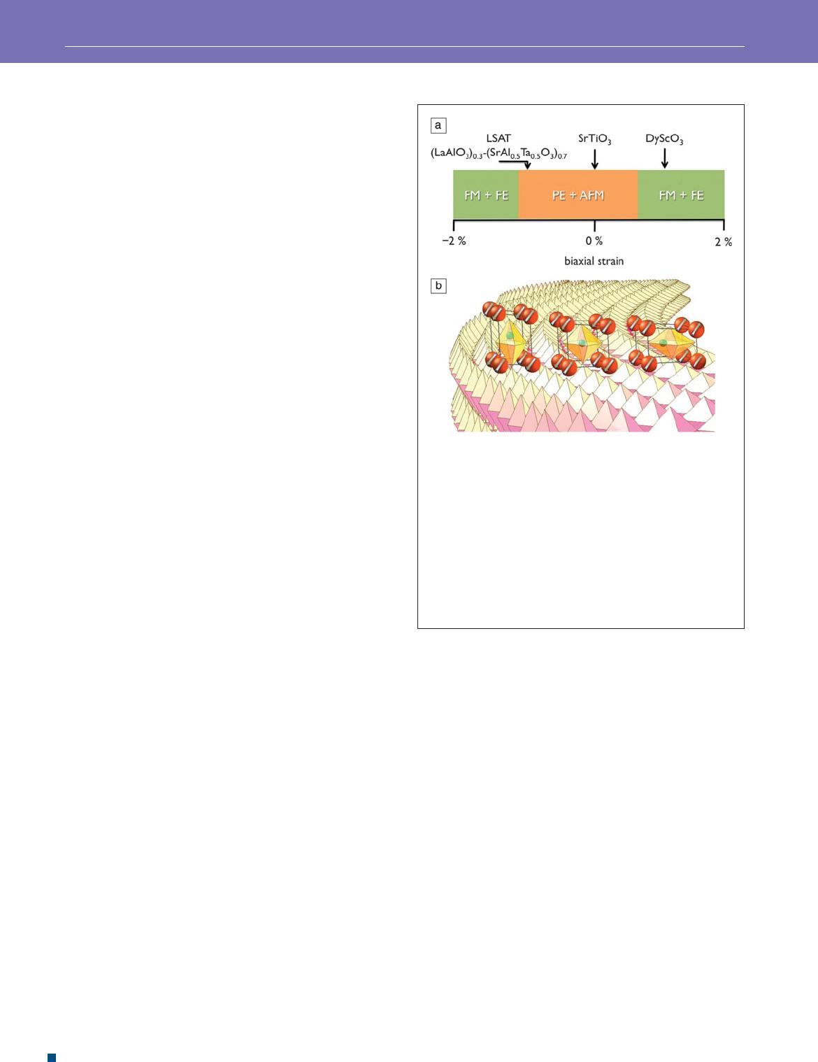
suggestions from computation. Figure 2 displays the computed
property phase diagram of strained EuTiO
3
as a function of
the strain and schemes of the resulting crystal and magnetic
structures. It should be noted that in these AB O
3
perovskites,
magnetism arises on the A site and polar behavior from the
displacement of the B ions.
The key role of formal theory: Development of
topological insulators
The discovery of three-dimensional topological insulators
provides an example of the interplay between different kinds
of theory and experiment and, in particular, emphasizes that for-
mal theory can play a key role in predicting and understanding
new phenomena. Materials-specifi c modeling, as embodied in
density functional electronic structure theory, can then play a
collaborating role in suggesting real systems where certain phe-
nomena may be observed. Interestingly, at a time when much
of condensed matter physics is focused on correlated electronic
phenomena, the understanding of topological insulators largely
requires simple, single-particle theories.
14
,
15
Topological insula-
tors are materials that are insulating in bulk but have protected
metallic surface states as a result of spin-orbit coupling. Formal
theoretical work, motivated by seeking generalizations of the
quantum Hall and quantum spin Hall effects in two-dimensional
systems, showed that similar mathematical structures (topologi-
cal invariants) could, in principle, be generated by spin-orbit
coupling, leading to new phases, dubbed topological insulators.
Several candidate materials were then proposed based on heu-
ristic arguments and fi rst-principles calculations, contributing
to the experimental discovery of the characteristic massless
surface state and spin-momentum locking in BiSb alloys and
Bi
2
Se
3
. This is an area that has been recently reviewed, for
example, in References 14 and 15. Following the initial role of
formal theory, more materials-specifi c approaches have come
into play, and a number of suggestions for interesting materials
classes have been put forth, such as the suggestion that the half-
Heusler XYZ structure type, comprising three interpenetrating
fcc sublattices of (usually) two metals, X and Y , and a main
group element, Z , is a rich playing fi eld for the area of tunable,
multifunctional topological insulators.
16
,
17
Better samples lead to new science: The
example of GaAs heterostructures
The science of topological insulators, referred to in the previous
section, is in fact closely inspired by studies on the fractional
quantized Hall effect. Single-crystal GaAs fi lms are a natural
extension of the deep experience of the scientifi c and techno-
logical community with single-crystal Si. A search by physi-
cists for a more perfect semiconductor-insulator interface than
realizable in Si-SiO
2
led to the development of the GaAs-AlAs
Figure 2. Suggestions from rst-principles electronic
structure calculations that perovskite EuTiO
3
can, under
both tensile and compressive strains, switch its ground state
from being paraelectric (PE) and antiferromagnetic (AFM)
to being ferroelectric (FE) and ferromagnetic (FM) have now
been experimentally realized. The upper panel (a) shows the
computed dependence of the ground state on strain, and the
lower panel (b) displays schemes of different magnetic and
polar orderings in the perovskite structure corresponding to the
regimes in (a). Orange atoms at the corners of the perovskite
cell are Eu
2+
and carry spin, indicated by arrows. TiO
6
octahedra
are indicated with Ti
4+
shown as green spheres at the centers
of the octahedra. Figure courtesy of Craig Fennie, Cornell
University.
ADVANCES IN FUNCTIONAL MATERIALS: TOWARD THE PARADIGM OF MATERIALS BY DESIGN
685
MRS BULLETIN
•
VOLUME 37
•
JULY 2012
•
www.mrs.org/bulletin
system, in which both the conducting GaAs and the insulating
AlAs are incorporated in the same single crystal, usually in
an alternating fashion. Using advances made in techniques
to epitaxially grow single-crystal fi lms, near-perfect crystal
interfaces can be produced. In these fi lms, the absence of a
disordered electronic interface gives the freedom to reduce the
conducting channel thickness to about 10 nm, which is near the
quantum size of conduction electrons in GaAs. The electrons
can thus move in the plane of the GaAs channel but not out of
the GaAs layer because of the AlAs insulating barriers. Thus,
a material that is effectively two-dimensional can be created.
The unusual nature of two-dimensional electrons can be
probed in Hall-effect experiments. For metal samples, such
as the gold leaf foil used originally by Edwin Hall in 1879, the
resistance grows smoothly and linearly with an increase in
the magnetic fi eld B. However, for high-purity semiconducting
systems at low temperatures, the Hall resistance shows a series
of discrete plateau steps that cannot be understood without
considering the quantum properties of the conducting electrons.
Even more striking is that the numerical values of the various
resistance plateaus are given by exact ratios of fundamental
physical constants, at values of h /( ν e
2
), where h is Planck’s
constant, e is the charge on the electron, and ν is the fi lling fac-
tor, which in the Quantum Hall Effect takes on integer values.
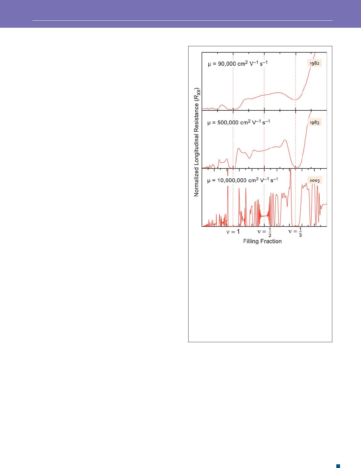
The realization that increasing the crystalline quality in the
two-dimensional region could lead to a more robust quantum
Hall effect led to experiments using the potentially higher-
quality GaAs-AlGaAs interface. In 1982, Stormer et al.
18
published a truly novel experimental result shown in the top
panel of Figure 3 . Not only did they see the integer effect,
but they also saw a clear plateau at ν = 1/3, in other words, a
fractional rather than an integer value. They had discovered
the fractional quantum Hall effect. This discovery in GaAs
launched an effort to further improve the quality of the GaAs
crystal samples. The panels in Figure 3 show the increasing
richness of observed fractional states as the sample quality
(measured by the electron mobility μ ) has improved over the
years. For a sample of mobility 5 × 10
5
cm
2
V
−1
s
−1
,
19
one sees that
the states at 1/3 and 2/3 are joined by other states, and in the
bottom-most trace where the mobility is of the order of 10
7
cm
2
V
−1
s
−1
,
20
these states are joined by a hierarchy of states, all hav-
ing odd denominators and all organized around an absent state
at ν = 1/2. These experiments provide dramatic evidence for a
series of new emergent particles called composite fermions.
21
Better samples lead to better understanding:
The example of SrTiO
3
and conducting polymers
One of the lessons learned from GaAs is the importance of
sample quality. This has recently become of particular relevance
in the examination of thin fi lms of high quality oxides and their
heterointerfaces that have so captured the imagination with the
possibility of oxide electronics.
22
The question of whether the
kinds of growth processes that are applicable in the prepara-
tion of high quality GaAs fi lms can be transferred to oxide thin
fi lms has recently been addressed.
23
Molecular beam epitaxy
of SrTiO
3
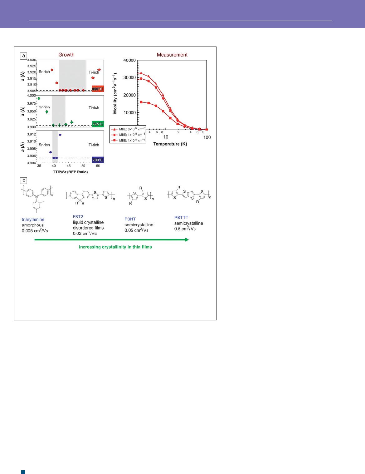
uses a molecular beam source for Sr and titanium
tetraisopropoxide (TTIP) for the Ti source. A key to growing
high quality fi lms is to work under conditions, also frequently
referred to as growth windows, which naturally lead to the cor-
rect stoichiometry of the phase being formed. In SrTiO
3
, this
is appropriately probed using the unit cell parameter. SrTiO
3
is an optimally bonded band semiconductor, and any change
from the “1-1-3” stoichiometry results in underbonding, as seen
from an expansion of the lattice. The growth windows therefore
correspond to regions where the lattice parameter displays a
plateau as a function of varying the ratio of starting materials,
and this plateau is a minimum. This is displayed in the left panel
of Figure 4 a.
23
The use of such a growth window has resulted
in complex oxide fi lms with unprecedented mobilities,
24
as seen
Figure 3. Better samples lead to new science: Longitudinal
resistance, R
xx
, for three different two-dimensional electron gas
samples as a function of the magnetic eld, as expressed in
terms of lling factor ν = nh / eB, where n is the electron density,
h is the Planck constant, e is the charge on an electron, and B
is the magnetic eld. The samples are formed at the interface of
crystalline GaAs and AlGaAs grown by molecular beam epitaxy.
The samples are distinguished by different values of the mobility,
μ , that have increased systematically over time. The upper frame
shows the rst report, in 1982, of fractional lling at ν = 1/3 and
T = 0.48 K.
18
The middle frame shows new states at ν = 1/3,
2/5, 2/3 achieved in higher mobility samples at T = 0.55 K.
19
The
bottom frame shows data from a typical modern high mobility
sample at T = 0.35 K.
20
This sample exhibits self similarity
between the ν = 0 and ν = 1/2 states that is the basis for the
“composite fermion” description of electronic states.
ADVANCES IN FUNCTIONAL MATERIALS: TOWARD THE PARADIGM OF MATERIALS BY DESIGN
686
MRS BULLETIN
•
VOLUME 37
•
JULY 2012
•
www.mrs.org/bulletin
in the right panel of Figure 4a . Complex oxides are fascinating
materials because of the range of physical phenomena that they
can display and, in bringing semiconducting oxides into this
high-mobility regime, what seems to be one of the last materials
frontiers is being traversed.
In the area of organic electronics, discussed in the next
section, the extent of delocalization is important in design-
ing the electronic properties of molecules. In addition, it is
also critical to think of the morphology and, specifi cally,
the extent of crystallinity in the case of evaporated fi lms. In
Figure 4b , the mobility, measured using fi eld-effect transistor
geometry, of some amorphous, liquid crystalline, and semi-
crystalline conjugated polymers are displayed. A clear trend
is observed that with increasing crystallinity, the mobil-
ity increases by two orders of magnitude. The availability
of organic polymer fi lms displaying increasingly higher
mobility and potentially band-like transport enables better
understanding and even modeling of these
highly complex systems. Comparing organics
with the oxides, and the more classical main
group semiconductors referred to previously,
it becomes evident that although the observed
phenomena can differ by many orders of
magnitude, some of the goals (e.g., the fab-
rication of transistors) in the very divergent
materials classes can be similar.
The organic advance of
optoelectronics: Light-emitters,
photovoltaics, and transistors
Organic materials hold a great deal of promise
for applications in electronic and optoelectronic
devices. Both molecular and polymeric materi-
als have several properties that make them well
suited to these applications. Both are readily
tailored by chemical substitution to grossly and
fi nely tune their electronic properties, includ-
ing fi lled and vacant state energies as well as
their absorption and excited state energies.
They can have conductivities ranging from as
low as those of the best wide gap insulators,
through semiconducting to metallic. Their
optical absorptivity can be significantly
larger than direct bandgap semiconductors,
with extinction coeffi cients as high as 10
6
cm
−1
. They can also be designed to emit with
high effi ciency, ranging in color from the UV
to the near-infrared. Lastly, both molecular
and polymeric materials can be peripherally
substituted to affect the mechanical and mor-
phological properties without signifi cantly
affecting the electronic properties of the
materials. This last property of organic mate-
rials is key to their future applications, as we
move toward organic materials by design, in
which the microscopic and macroscopic properties of the
compounds are tailored independently to achieve the optimal
materials for each application.
The fi rst organic optoelectronic device to go into full-scale
production was the organic light-emitting diode (OLED), and
signifi cantly more manufacturing capacity is being planned and
added at this time. Electroluminescence in organic materials has
been known since the mid-1960s.
25
,
26
However, the demonstra-
tion of the fi rst heterostructured OLEDs in the late 1980s set
the stage for major advances in effi ciencies and color tunability
of these devices.
27
,
28
By carefully controlling charge injec-
tion and recombination as well as the site of light emission in
OLEDs, internal effi ciencies have improved from ca. 5% in
1987 to 100% in the early part of this century.
29
–
32
The rapid
development of OLEDs, from a laboratory demonstration
to a commercial product, involved the dedicated work of a
broad range of scientists and engineers working together to both
Figure 4. Better samples lead to better understanding. (a) The left panel displays the
existence of growth of windows (shaded regions) in the hybrid molecular beam epitaxy
(MBE) growth stoichiometric SrTiO
3
as monitored from the cubic unit cell parameter
a .
23
The horizontal axis displays the beam equivalent pressure (BEP) ratio of titanium
tetraisopropoxide (TTIP) to strontium. The right panel displays the record mobilities that
become achievable from the lms grown in these growth windows.
24
Figure courtesy of
Susanne Stemmer. (b) Improved crystallinity in semiconducting polymer lms results in
signi cantly increased mobilities, as measured using a eld-effect transistor geometry.
Figure courtesy of Michael Chabinyc. R, generic organic group; S, sulfur; N, nitrogen;
n , an integer; F8T2, dioctyl uorene-bithiophene; P3HT, poly(3-hexylthiophene);
PBTTT, poly(2,5-bis(3-alkylthiophen-2-yl)thieno[3,2- b ]thiophene).

ADVANCES IN FUNCTIONAL MATERIALS: TOWARD THE PARADIGM OF MATERIALS BY DESIGN
687
MRS BULLETIN
•
VOLUME 37
•
JULY 2012
•
www.mrs.org/bulletin
understand and improve electroluminescent devices. The solu-
tions that were developed involved the use of thin amorphous
fi lms. Materials need to be amorphous to achieve acceptable fi lm
uniformity for the 10 nm to 40 nm fi lms that are used in OLEDs.
These fi lm thicknesses are necessary to keep the resistivity of the
device low enough to achieve low drive voltages. Manufactur-
ing these devices would be easier, and the power effi ciencies of
the devices would be improved if we could increase fi lm thick-
ness and decrease fi lm resistivity, respectively. While these two
goals seem mutually exclusive, if crystalline thin fi lms—some of
which are shown in Figure 4b —could be used for OLED prepa-
ration, it could be possible to both increase fi lm thickness and
decrease resistivity. Beyond simply growing uniform crystalline
fi lms, it is important to be able to predetermine the orientation
of the lattice to maintain maximum conductivity in the desired
direction, parallel or perpendicular to the substrate. Two other
existing devices could benefi t from such a level of materials
design and control: photovoltaics and transistors.
Organic solar cells have the potential to achieve high effi -
ciency for conversion of sunlight into electricity at a cost
well below existing solar technologies. Organic photovoltaics
(OPVs) with effi ciencies exceeding 10% have been certifi ed
by the National Renewable Energy Laboratory,
33
although
the structures have not been published. Effi ciencies of >25%
are possible for single junction cells.
34
While the OPV is in
many ways the microscopic inverse of the OLED, there are
important differences between the two. The high resistivity of
organic materials can be tolerated in an OLED, because very
thin fi lms could be used to minimize the bias needed to inject
and transport charge in the devices. If such thin fi lms are used
in OPVs, the problem of resistivity is minimized, but the fi lms
are so thin that very little light is absorbed. Thus, in an OLED,
it is possible to restrict all light emission to a very thin fi lm,
typically less than 30 nm, while in an OPV, the light absorption
must be spread over a much larger volume to achieve good
light collection. The most effi cient OPVs are those that use
thermal or solvent annealing to achieve a degree of crystallin-
ity in the organic materials. This is often done with donor (D)
and acceptor (A) materials in an interpenetrating network to
effi ciently collect excitons (i.e., the bulk heterojunction, BHJ),
since simple layered devices give exciton diffusion lengths that
are too short to give effi cient collection at the D/A interface.
This is again a technology that would be well served by being
able to control fi lm crystallinity and morphology over a large
area. Crystalline materials will have lower resistivity and higher
exciton diffusion lengths than the amorphous or polycrystalline
materials that are used currently. If it were possible to grow
highly crystalline thin fi lms of organic materials, with the pre-
ferred orientation of the organic moieties to direct excitons to
the D/A interface and charges out the electrodes, OPVs could
be fabricated with simple layered structures, rather than BHJs,
and achieve effi ciencies closer to the 25% theoretical limit.
35
Organic fi eld-effect transistors, OFETs, have advanced tre-
mendously over the last decade.
36
,
37
A key limitation of OFETs is
the carrier mobilities of organic materials. While values higher
than 1 cm
2
V
−1
s
−1
have been reported for organic materials, these
are still many orders of magnitude below those seen for inor-
ganic semiconductors, including GaAs and SrTiO
3
mentioned
earlier. The highest mobilities, and thus the best transistor per-
formance, are observed for single-crystalline materials. An
approach to using such materials in OFETs involves thermal
annealing to achieve crystalline grains that are larger than the
channel length.
The key to improving the effi ciencies of organic electronic
and optoelectronic devices is to develop the methodology to
grow organic materials in predetermined structures and orienta-
tion in large area thin fi lms. To develop this capability, it will
take a multidisciplinary and consistent effort. This will start
with theorists. It is possible to calculate many molecular param-
eters and even the bulk properties of a material in a given struc-
ture, to a limited degree. It has not been possible, however, to
reliably predict the morphology an organic material will adopt
in the solid state. In order to create methodologies for crystal-
line organic fi lm growth, it is important to couple researchers in
theoretical modeling with experimentalists to develop models
that effectively deal with both kinetic and thermodynamic
parameters to predict the structures of organic thin fi lms.
The fi rst step is to develop deposition tools that allow the
researcher to accurately control the deposition and growth
parameters for the organic thin fi lm, from both solution and
vapor sources. Next, theorists and experimentalists need to
work together to design, synthesize, and study the deposition
of molecules that are predicted to give preferred structures
under a set of deposition conditions. Materials that fail to
give the expected structure can be used to refi ne the model
and develop the deposition techniques further, so there are
no real failures in this approach. Working through this cycle
many times should provide a set of design parameters that
can be used to control the morphologies and properties of
organic thin fi lms.
New directions in nanoscience
The fi eld of nanomaterials has progressed considerably
since its emergence as a distinct discipline from cluster
and colloid science some 30 years ago. Advances have
been spurred by new chemistry knowledge as well as
new physical techniques and/or greater access to appro-
priate physical techniques (e.g., electron microscopy,
atomic force microscopy). At the present stage of devel-
opment, syntheses exist for a range of nanomaterials, mostly
single-element phases or binaries. This is in contrast to the
better-developed solid-state chemistry discipline, where
highly complex materials—ternary, quaternary materials
and beyond, and defect or dopant controlled materials—are
at the forefront of science. With the excellent foundation of
the past three decades of research, the fi eld of nanomaterials
is now poised to tackle a range of technical challenges. This
includes the synthesis of new, more complex materials, better
methods for nanoparticle integration, more detailed physical
characterization of existing materials (wherein new phenomena

ADVANCES IN FUNCTIONAL MATERIALS: TOWARD THE PARADIGM OF MATERIALS BY DESIGN
688
MRS BULLETIN
•
VOLUME 37
•
JULY 2012
•
www.mrs.org/bulletin
can be found), combined theoretical/experimental approaches
to understand nanoscale phenomena, and the deployment of
nanomaterials in device architectures.
The rich phase diagrams established for solid-state materials
provide a great source of new material compositions to be
targeted on the nanoscale, both as homogeneous (alloys or com-
pounds) and heterogeneous (e.g., core-shell) architectures. The
formation of homogeneous structures of ternary phases has been
achieved by direct synthesis from multicomponent solutions or
from chemical transformations.
38
Likewise, the ability to tune
the electro-optical properties of quantum dots by overcoating
with a semiconductor of a different bandgap, or the creation
of multifunctional structures by combining mutually exclusive
properties (e.g ., magnetism and photoluminescence) into a single
nanostructure
39
,
40
have proven to be powerful paradigms in nano-
material design. Structure-property-size correlations in complex
nanomaterials will be a fruitful area of exploration for some time
to come, driven by improved synthetic methods that enable high
quality nanocrystals and nanocomposites to be generated.
Doping or the introduction of defects into bulk solids is an
established method for tuning the optoelectronic properties,
but doping on the nanoscale has proven to be a complex prob-
lem, restricting the kinds of phenomena that can be accessed in
such materials. This problem has been addressed by a com-
bination of experimental and theoretical approaches,
41
which
revealed the key issue to be low binding energies for dopant
ions on certain crystalline faces. If the residence time is not
suffi cient for host layer overgrowth (i.e ., incorporation), low
to zero incorporation occurs. A key advantage of this “trapped
dopant” model is that binding energies for ions and competing
surfactants can be calculated for distinct facets, enabling doping
to be enhanced by appropriate solvent choices and/or crystallite
morphologies. Exploitation of this insight enables the effect
of coupling of size and doping on the nanoscale to be probed, for
example, the effects of quantum confi nement effects on magnetic
semiconductors. Combining theory with experiment is also shed-
ding light on physical phenomena, as demonstrated by the appli-
cation of d -band theory to the prediction of catalyst performance
42
or the modeling of interface scattering to predict optimal grain
sizes in thermoelectric nanocomposites.
43
The synergy that arises
when experiment and theory act in a feedback loop enables the
rational construction of nanomaterials for targeted applications.
Employing nanoparticles as discrete components for med-
ical applications based on optical and magnetic properties
was an early focus of investigation and continues apace.
The integration of nanomaterials into electronic devices,
of particular relevance for energy applications (photovolta-
ics, thermoelectrics, and batteries), has progressed more
slowly, as it is predicated on conductive particle interfaces.
Methods that generate well-formed discrete nanoparticles
typically produce materials with long-chain organics on the
surface, preventing facile transport of electrons. Advances
have been made by the use of conducting ligands,
44
ligands
that are thermally labile ( t -butylthiol),
45
replacement of organic
ligands with inorganic ligands such as molecular chalcogenide
clusters,
46
sulfi de,
47
or hydrazine,
48
and use of ligand removal
coupled to direct inter-particle bonding (sol-gel particle assem-
bly).
49
A consequence of such modifi cations is changes in sur-
face defects that modify luminescence characteristics and the
potential reduction in quantum confi nement in semiconduc-
tors. Alternative approaches focus on building nanostructures
directly from molecular building blocks, generating gels or
templated solids and obviating the need for ligand modifi cation
strategies altogether.
50
The role of serendipity: New inorganic pigments
from the search for multiferroics
In Horace Walpole’s 1754 retelling of a Persian fairy tale, three
well-raised princes from Serendip—modern-day Sri Lanka—
are continually making discoveries of things they are not in
quest of. The word that has emerged into common currency
from this tale, serendipity, is used to suggest the act of fi nding
something useful without really looking for it, or even perhaps
without prior knowledge of its existence. Modern materials sci-
ence is a chronicle of serendipitous discovery exemplifi ed by the
original discovery of superconductivity by Kamerlingh-Onnes,
the discovery in 1938 of polytetrafl uoroethylene (Tefl on) by Roy
Plunkett of DuPont Company, or the recent discovery of super-
conductivity in layered transition metal pnictides by the Hosono
group at the Tokyo Institute of Technology, who were in fact
searching for new transparent conductors.
51
In this regard, we
emphasize the importance of exploratory synthesis in materials
research, whose purpose is to escape the intellectual confi nes of
what we know in order to discover the new and the unexpected.
The recent discovery of highly durable and non-toxic inor-
ganic color pigments in oxides with transition metal cations in
trigonal bipyramidal (TBP) coordination can be considered as a
textbook example of how a systematic approach to discover new
functional materials in one area can lead to a totally unexpected
discovery in another, unrelated area. Both YInO
3
and YMnO
3
are known in the common orthorhombic and centrosymmetric
perovskite structure, but they are also readily prepared in an
acentric hexagonal structure ( Figure 5 , left panel),
52
,
53
consisting
of layers of Y
3+
ions separating layers of corner-shared M O
5
trigonal bipyramids ( M = In or Mn). This structure has been
of considerable recent interest because it exhibits an unusual
form of improper ferroelectricity (meaning the ferroelectric
polarization is not the primary driving force for the structural
change) as a consequence of the tilting of MO
5
polyhedra.
54
,
55
Such ferroelectricity is compatible with M -site magnetism and
therefore allows multiferroic behavior. To explore such multi-
ferroic behavior, the complete YIn
1− x
Mn
x
O
3
solid solution was
prepared. Despite the large size mismatch between In
3+
and
Mn
3+
, these cations are randomly disordered in the TBP sites.
56
Unfortunately, such a disorder suppresses the multiferroic order
parameter, rendering the system unsuitable for applications as a
magnetoelectric material.
57
However, a surprisingly intense and
bright blue pigment is obtained when Mn
3+
is introduced into the
trigonal bipyramidal sites in hexagonal YInO
3
, and over much of
the YIn
1− x
Mn
x
O
3
solid solution range, in spite of the fact that YInO
3

ADVANCES IN FUNCTIONAL MATERIALS: TOWARD THE PARADIGM OF MATERIALS BY DESIGN
689
MRS BULLETIN
•
VOLUME 37
•
JULY 2012
•
www.mrs.org/bulletin
and YMnO
3
are white and black, respectively. An intense blue
color is also obtained when Mn
3+
is introduced into trigonal bipy-
ramidal sites in other oxides. These unexpected discoveries have
led to the rational design of other earth-abundant, environmentally
benign and highly durable inorganic pigments. Substitution of Fe
3+
in hexagonal YInO
3
resulted in the formation of intense orange
compounds,
58
whereas the simultaneous substitution of Cu
2+
and
Ti
4+
along with Al
3+
in TBP sites resulted in the formation of oxides
exhibiting intense green color.
59
Serendipitous discoveries require intellectual effort and are not
simply a question of luck, and, indeed, we hark back to the tale
that tells us that the princes were actually well trained to observe
and interpret whatever they happened upon. Unpredictable results
and discoveries are as much a part of scientifi c endeavor, but ser-
endipity manifests when the alert and trained mind responds to
an unexpected situation. Basic exploratory research necessarily
incorporates serendipity, and thus sustained support for exploratory
research should not be neglected.
Conclusions
The systematic search for new functional materials specifi cally
designed to address existing challenges of technology has seen
a recent and well-deserved surge of attention. In particular,
the need to fi ll the materials discovery gap engendered by the
shrinking of once-prolifi c industrial laboratories
1
and the need
(and the necessary means) for approaches that can speed up
the arc from discovery to technology
3
have been emphasized.
In this article, we have simultaneously pointed to the needs
in some emerging areas as well as the requirements for better
Figure 5. (a) Crystal structure of polar, hexagonal YMnO
3
displaying the B cation (Mn
atoms here) in a trigonal bipyramidal environment, indicated by the blue polyhedra. Orange
spheres represent O atoms, and the dark gray spheres represent Y atoms. (b) Examples of
oxide pigments prepared by appropriate substitution of transition metal ions into trigonal
bipyramidal coordination.
materials that can enable new science. The
consensus that is emerging is that in areas
where a targeted search for better materials
is necessary, there is a need for strong col-
laboration between theory and experiment at
every level. At the same time, history tells
us that exploratory research and the abil-
ity to be surprised should continue to play
an important role and should be supported
appropriately.
Acknowledgment
We are very grateful to the National Science
Foundation (DMR 1115294) for support-
ing the Materials by Design Workshop, and
especially to Drs. Linda Sapochak and Daniele
Finotello for their support and encouragement.
We thank all the participants of the Workshop
for their many useful and creative inputs,
and acknowledge Michael Chabinyc, Craig
Fennie, John Mitchell, Joel Moore, Susanne
Stemmer, and Pat Woodward for providing
us with fi gures and explanations.
References
1 . Frontiers in Crystalline Matter: From Discovery to
Technology, Committee for an Assessment of and Outlook
for New Materials Synthesis and Crystal Growth ( National Research Council ,
2009 ).
2 . Materials Genome Initiative for Global Competitiveness ( White House Offi ce
of Science and Technology Policy , 2011 ) p. 6 .
3. G.R. Fleming , M.A. Ratner , Phys. Today 61 ( 7 ), 28 ( 2008 ).
4. J. Gertner , “ Innovation and the Bell Labs Miracle ,” New York Times (February
25, 2012 ).
5. W.C. Johnson , J.B. Parsons , M.C. Crew , J. Phys. Chem. 36 , 2651 ( 1932 ).
6. R. Juza , H. Hahn , Z. Anorg. Allg. Chem. 239 , 282 ( 1938 ).
7. E.F. Schubert , Light Emitting Diodes, 2nd ed. ( Cambridge University Press ,
UK , 2006 ).
8. S. Nakamura , T. Mukai , M. Senoh , Appl. Phys. Lett. 64 , 1687 ( 1994 ).
9. S. Nakamura , M. Senoh , S. Nagahama , N. Iwasa , T. Yamada , T. Matsushita ,
H. Kiyoku , Y. Sugimoto , Jpn. J. Appl. Phys. 35 , 74 ( 1996 ).
10. N.A. Spaldin , M. Fiebib , Science 309 , 391 ( 2005 ).
11. T. Kimura , Annu. Rev. Mater. Res. 37 , 387 ( 2007 ).
12. C.J. Fennie , K.M. Rabe , Phys. Rev. Lett. 97 , 267602 ( 2006 ).
13. J.H. Lee L. Fang , E. Vlahos , X. Ke , Y.W. Jung , L. Fitting Kourkoutis , J.W. Kim ,
P. Ryan , T. Heeg , M. Roeckerath , V. Goian , M. Bernhagen , R. Uecker , C. Hammel ,
K.M. Rabe , S. Kamba , J. Schubert , J.W. Freeland , D.A. Muller , C.J. Fennie , P. Schiffer ,
V. Gopalan , E. Johnston-Halperin , D.G. Schlom , Nature 466 , 954 ( 2010 ).
14. J.E. Moore , Nature 464 , 194 ( 2010 ).
15. M.Z. Hassan , C.L. Kane , Rev. Mod. Phys. 82 , 3045 ( 2010 ).
16. S. Chadov , X. Qi , J. Kübler , G.H. Fecher , C. Felser , S.C. Zhang , Nat. Mater.
9 , 541 ( 2010 ).
17. H. Lin , L.A. Wray , Y. Xia , S. Xu , S. Jia , R.J. Cava , A. Bansil , M.Z. Hassan ,
Nat. Mater. 9 , 546 ( 2010 ).
18. D.C. Tsui , H.L. Stormer , A.C. Gossard , Phys. Rev. Lett. 48 , 1559
( 1982 ).
19. H.L. Stormer , A. Chang , D.C. Tsui , J.C.M. Hwang , A.C. Gossard , W. Wiegmann ,
Phys. Rev. Lett.
50 , 1953 ( 1983 ).
20. W. Pan , H.L. Stormer , D.C. Tsui , L.N. Pfeiffer , K.W. Baldwin , K.W. West , Phys.
Rev. Lett. 90 , 16801 ( 2003 ).
21. J.K. Jain , Phys. Rev. Lett. 63 , 199 ( 1989 ).
22. H.Y. Hwang , Y. Iwasa , M. Kawasaki , B. Keimer , N. Nagaosa , Y. Tokura , Nat.
Mater. 11 , 103 ( 2012 ).
23. B. Jalan , P. Moetakef , S. Stemmer , Appl. Phys. Lett. 95 , 032906 ( 2009 ).
24. J. Son , P. Moetakef , B. Jalan , O. Bierwagen , N.J. Wright , R. Engel-Herbert ,
S. Stemmer , Nat. Mater. 9 , 482 ( 2010 ).
25. M. Pope , H.P. Kallmann , P. Magnante , J. Chem. Phys. 38 , 2042 ( 1963 ).

ADVANCES IN FUNCTIONAL MATERIALS: TOWARD THE PARADIGM OF MATERIALS BY DESIGN
690
MRS BULLETIN
•
VOLUME 37
•
JULY 2012
•
www.mrs.org/bulletin
26. W. Helfrich , W.G. Schneidere , Phys. Rev. Lett. 14 , 229 ( 1965 ).
27. W. Helfrich , W.G. Schneidere , J. Chem. Phys. 14 , 2902 ( 1965 ).
28. C.W. Tang , S.A. VanSlyke , Appl. Phys. Lett. 51 , 913 ( 1987 ).
29. C.W. Tang , S.A. VanSlyke , J. Appl. Phys. 65 , 3610 ( 1989 ).
30. H. Yersin , Ed., Highly Effi cient OLEDs with Phosphorescent Materials ( Wiley-
VCH , Berlin , 2007 ).
31. M.E. Thompson , P.E. Djurovich , S. Barlow , S.R. Marder , in Comprehensive
Organometallic Chemistry III , R.H. Crabtree , D.M.P. Mingos , Eds. ( Elsevier ,
Oxford, UK , 2007 ), Chapter 12.04.
32. L. Flamigni , A. Barbieri , C. Sabatini , B. Ventura , F. Barigelletti , Top. Curr.
Chem. 281 , 143 ( 2007 ).
33. http :// www . nrel . gov / ncpv / images / effi ciency_chart . jpg
34. C. Ulbricht , B. Beyer , C. Freibe , A. Winter , U.S. Schubert , Adv. Mater. 21 ,
4418 ( 2009 ).
35. N.C. Giebink , G.P. Wiederrecht , M.R. Wasielewski , S.R. Forrest , Phys. Rev. B
83 , 195326 ( 2011 ).
36. M. Małachowski , J. Ľmija , Opto-Electron. Rev. 18 , 121 ( 2010 ).
37. W. Wu , Y. Liu , D. Zhu , Chem. Soc. Rev. 39 , 1489 ( 2010 ).
38. Y. Vasquez , A.E. Henkes , J.C. Bauer , R.E. Schaak , J. Solid State Chem. 181
1509 ( 2008 ).
39. H. Kim , M. Achermann , L.P. Balet , J.A. Hollingsworth , V.I. Klimov , J. Am. Chem.
Soc. 127 , 544 ( 2005 ).
40. F.X. Redl , K.-S. Cho , C.B. Murray , S. O’Brien , Nature 423 , 968 ( 2003 ).
41. S.C. Erwin , L. Zu , M.I. Haftel , A.L. Efros , T.A. Kennedy , D.J. Norris , Nature
436 , 91 ( 2005 ).
42. E. Nikolla , J. Schwank , S. Linic , J. Am. Chem. Soc. 131 , 2747 ( 2009 ).
43. A. Popescu , A. Datta , G.S. Nolas , L.M. Woods , J. Appl. Phys. 109 , 103709 ( 2011 ).
44. D.J. Milliron , A.P. Alivisatos , C. Pitois , C. Edder , J.M.J. Fréchet , Adv. Mater.
15 , 58 ( 2003 ).
45. D.H. Webber , R.L. Brutchey , J. Am. Chem. Soc.
134 , 1085 ( 2012 ).
46. M.V. Kovalenko , M. Scheele , D.V. Talapin , Science 324 , 1417 ( 2009 ).
47. H. Zhang , B. Hu , L. Sun , R. Hovden , F.W. Wise , D.A. Muller , R.D. Robinson ,
Nano Lett. 11 , 5356 ( 2011 ).
48. J.J. Urban , D.V. Talapin , E.V. Shevchenko , C.B. Murray , J. Am. Chem. Soc.
128 , 3248 ( 2006 ).
49. J.L. Mohanan , I.U. Arachchige , S.L. Brock , Science 307 , 397 ( 2005 ).
50. D.R. Rolison , L.F. Nazar , MRS Bull. 36 , 486 ( 2011 ).
51. Y. Kamihara , H. Hiramatsu , M. Hirano , R. Kawamura , H. Yanagi , T. Kamiya ,
H. Hosono , J. Am. Chem. Soc. 128 , 10012 ( 2006 ).
52. A. Waintal , J. Chenavas , C.R. Acad. Sci. Paris 264 ( 1967 ).
53. C.W.F.T. Pistorius , J.G. Kruger , J. Inorg. Nucl. Chem. 38 , 1471 ( 1976 ).
54. B.B. Van Aken , A. Meetsma , T.M. Palstra , Acta Crystallogr. C 57 , 230 ( 2001 ).
55. B.B. Van Aken , T.M. Palstra , A. Filippetti , N.A. Spaldin , Nat. Mater. 3 , 164 ( 2004 ).
56. A.E. Smith , H. Mizoguchi , K. Delaney , N.A. Spaldin , A.W. Sleight ,
M.A. Subramanian , J. Am. Chem. Soc. 131 , 17084 ( 2009 ).
57. A. Dixit , A.E. Smith , M.A. Subramanian , G. Lawes , Solid State Commun.
150 , 746 ( 2010 ).
58. P. Jiang , J. Li , A.W. Sleight , M.A. Subramanian , Inorg. Chem. 50 , 5858 ( 2011 ).
59. A.E. Smith , A.W. Sleight , M.A. Subramanian , Mater. Res. Bull. 46 , 1 ( 2011 ).
Ram Seshadri is a professor in the Materials
Department and in the Department of Chemistry
and Biochemistry at the University of California,
Santa Barbara (UCSB). He received his BS degree
in chemistry from St. Stephens College, Delhi, in
1989, and his PhD degree in solid-state chemistry
from the Indian Institute of Science, Bangalore, in
1995. After some years as a postdoctoral fellow in
Caen, France, and Mainz, Germany, he started a
faculty career as an assistant professor in
Bangalore in 1999, before moving to UCSB in
2002. Seshadri’s research program addresses
structure-composition-property relations in
functional inorganic materials, focusing currently
on magnetic and correlated materials, catalysts, and phosphors. Seshadri can be
reached at the Materials Department and the Department of Chemistry and
Biochemistry, Materials Research Laboratory, University of California, Santa Barbara,
CA, USA; tel. 805-893-6129; and email [email protected] .
Stephanie L. Brock is a professor in the
Department of Chemistry at Wayne State
University. She received her BS degree in
chemistry from the University of Washington in
1990 and her PhD degree in chemistry from the
University of California, Davis, in 1995. From
1995 to 1999, she was a postdoctoral associate
at the University of Connecticut working on
nanoscale manganese oxide materials. Brock’s
research focuses on the synthesis, properties, and
applications of metal pnictide and chalcogenide
nanomaterials; the development of sol-gel
nanoparticle assembly methods and their
application to non-traditional materials; and
establishment of novel hybrid organic/inorganic nanomaterials for optoelectronic
and drug-delivery applications. Brock can be reached at the Department of
Chemistry, Wayne State University, Detroit, MI, USA; tel. 313-577-3102; and
email [email protected] .
Arthur P. Ramirez joined the University of
California, Santa Cruz, as dean of the Baskin
School of Engineering in May 2009 from LGS,
a subsidiary of Alcatel-Lucent. He earned his
BS and PhD degrees in physics at Yale University.
Ramirez spent much of his career at AT&T
Bell Laboratories, where he served as the
director of the device physics research department
before becoming leader of composite materials
and device development for LGS. His research
interests include frustrated systems, multiferroic
magnetic materials, and organic semiconduc-
tors. Ramirez can be reached at the Baskin
School of Engineering, University of California,
Santa Cruz, CA, USA; tel. 831-459-2158; and email [email protected] .
M.A. Subramanian is the Milton Harris Professor
of Materials Science at Oregon State University.
He received his BS and MS degrees from the
University of Madras, and his PhD degree from
the Indian Institute of Technology, Madras, in
1981. Following postdoctoral research at Texas
A&M University (1982–1984), Subramanian
joined Central Research & Development at
DuPont, where he remained until his recent
appointment at Oregon State. His research
interests include designing new inorganic
solid-state functional materials for emerging
applications in electronics, solid-state energy
conversion, and other areas. Subramanian can be
reached at the Department of Chemistry, Oregon State University, Corvallis, OR,
USA; tel. 541-737-8235; and email [email protected] .
Mark E. Thompson is a professor of chemistry
and materials science at the University of
Southern California (USC). He received his BS
degree in 1980 from the University of California,
Berkeley, and his PhD degree in 1985 from the
California Institute of Technology—both in
chemistry. After two years as a postdoctoral
fellow at Oxford University, he accepted a position
as an assistant professor in the Chemistry
Department at Princeton University. Thompson
joined USC in 1995. His research program
involves the study of new materials and devices
for electroluminescence, solar energy conversion,
chemical/biological sensing, and catalysis.
Thompson can be reached at the Department of Chemistry, University of
Southern California, Los Angeles, CA 90089, USA; tel. 213-704-6402; and
email [email protected] .
