Impact of Nonuniformities on Thin Cu(In,Ga)Se
2
Solar Cell Performance
Ana Kanevce, and James R. Sites
Physics Department, Colorado State University, Fort Collins, CO, 80523
ABSTRACT
Solar-cell performance degradation due to physical nonuniformities becomes more
significant as the thickness of polycrystalline absorbers is reduced. ìVoltageî nonuniformities
such as those due to band-gap fluctuations, variations in the back-contact proximity, and areas
where the absorber is completely depleted can have very significant impact on cell performance.
Similarly local shunts can seriously degrade the efficiency. ìCurrentî nonuniformities such as
optical defects have generally much less impact. The analysis presented is based on
Cu(In,Ga)Se
2
cells, but the qualitative results should be applicable to thin-absorber devices in
general. For lateral nonuniformity studies, the solar cell is simulated by a two dimensional
network of parallel diodes separated by resistors. The nonuniformities are approximated by
small regions of reduced photovoltage, often referred to as ìweak diodesî, and by isolated shunt
resistors. The weak-diode approach allows investigation of device performance as a function of
the weak-diode voltage deficit, the ratio of weak-to strong-diode area, and the weak diodesí
spatial distribution. Increased TCO resistance can isolate weak diodes, thus limiting the voltage
loss due to nonuniformities, but increasing fill-factor losses.
INTRODUCTION
Solar cells based on Cu(In,Ga)Se
2
(CIGS) are the most efficient thin-film polycrystalline
cells to date, with record efficiency of 19.5% [1, 2]. In the last few years, motivated by the
limited availability of the element In and by the need to decrease the production cost, several
groups have produced CIGS absorbers thinner than 1 µm [3-5]. Thinning the absorbers is
economically viable only if respectable conversion efficiency is maintained. To minimize the
losses, it is important to analyze the impact of nonuniformities on submicron absorbers. Thin-
absorber devices typically have smaller grain size. Variations in grain structure can significantly
affect device parameters and are likely more pronounced for submicron cells. Smaller grains
generally mean smaller carrier lifetime and may be more susceptible to band-gap fluctuations. In
addition to likely being less uniform, thinner CIGS performance is likely to be more sensitive to
uniformity fluctuations [6].
Nonuniformities in thin-film cells have been observed with several experimental
techniques, and these are reviewed in Ref. [7]. Previous nonuniformity studies [8-11] have
shown that potential fluctuations in CIGS cells are unavoidable and generally detrimental to the
cell performance. They also predict that a local series resistance, like the resistance of i-ZnO
layer, can reduce the nonuniformity losses. With a goal to minimize losses in submicron
devices, this work separates the physical causes for potential variations and analyzes which types
of nonuniformities impact thin devices more severely. It connects the sheet resistance of the
TCO with a single-diode series resistance and shows the impact on nonuniform device
efficiency.
Other studies have calculated the impact of a ìweak diodeî in a medium of stronger
neighbors [7, 12-14]. The distance over which the influence of weak diodes and shunts can be
Mater. Res. Soc. Symp. Proc. Vol. 1012 © 2007 Materials Research Society 1012-Y08-02
felt (screening length) depends on the transparent-conductive oxide (TCO) resistance.
Here the screening-length results are confirmed, and the weak-diode approach is extended to
determine the impact of low-voltage areas or shunts on the cellsí J-V parameters, and how the
distribution of week diodes affects the magnitude of performance loss.
PARAMETER SENSITIVITY
Submicron-device performance is in general sensitive to variations in material and
structural parameters. Thickness fluctuations impact submicron devices to a greater degree, and
in the extreme case, with fluctuations comparable to the absorber thickness, they can lead to
shunting. The impact on the solar cell parameters of band-gap fluctuations, however, should be
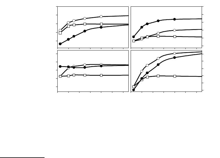
thickness independent [6]. Simulation results showing the change of two other solar-cell
parameters with thickness are shown in figure 1. In the baseline case (17.1% efficiency at 1 µm)
shown with circles, the minority-carrier lifetime in the absorber is 1 ns and the hole density is 2 x
10
16
cm
-3
. Thicknesses less than 1 µm decrease all three solar-cell parameters, and these
decreases become steeper for thickness below 500 nm. Roughness will therefore have stronger
effect on the lowest thickness devices. The calculated performance of a device with an order of
magnitude lower lifetime (squares in figure 1) shows less pronounced thickness dependence,
except for extremely low thicknesses (< 400 nm). The minority-carrier lifetime actually has
stronger effect on thicker devices due to their larger recombination volume. Lower hole-density
(dots in figure 1) decreases the voltage, but increases the current by about the same fraction.
V
oc
[V]
0.50
0.55
0.60
0.65
0.70
J
sc
[mA/cm
2
]
30
32
34
36
38
40
absorber thickness [µm]
0.2 0.4 0.6 0.8 1.0 1.2 1.4
FF
0.65
0.70
0.75
0.80
0.85
absorber thickness [µm]
0.2 0.4 0.6 0.8 1.0 1.2 1.4
Efficiency [%]
12
13
14
15
16
17
τ = 1 ns, p = 2 X 10
16
cm
-3
0.1; 2 X 10
16
1; 2 X 10
15
good cell reduced p
reduced τ
Figure 1. Calculated impact of absorber thickness on high-efficiency cell parameters (circles).
Corresponding results with reduced lifetime (squares) and reduced carrier density (dots) also
shown.
2) WEAK-VOLTAGE FRACTION IN A SOLAR CELL
2.a) The model
For a nonuniform device, the equivalent circuit for a single diode is replaced here with a
network of diodes that may be individually defined. The numerical simulations in this work use
a 10 x 10 diode network, part of which is shown in figure 2. The baseline ìstrong diodeî has V
oc
= 0.64 V, J
sc
= 34.2 mA/cm
2
, FF = 78% and η = 17.1 %, similar to values that have been
reported for 1-µm CIGS absorbers [5]. The back-contact resistance is neglected, and the grid-
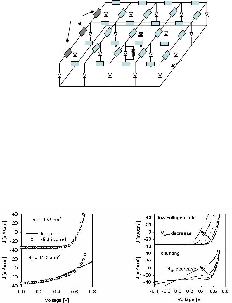
line resistance is taken to be 30 mΩ, negligible compared to the transparent-conductive oxide
(TCO) front-contact resistance.
The resistance R (distributed resistance) between the individual diodes is proportional to
the series resistance R
s
of the whole solar cell [15, 16]. The conversion coefficient depends on
the geometry of the device, and for the array used here an individual resistance of R = 3 Ω
corresponds to series resistance of R
s
= 1 Ω-cm
2
for the whole cell.
Figure 2. Schematic of diode network model. Single weak diode and shunt are highlighted.
The impact of a weak diode and a shunt on J-V curves is shown on figure 4.
The conversion between R and R
s
works well for low TCO resistances, but not so well
for higher ones (figure 3). The disagreement between the curves increases with increased
voltage bias, and for reasonable R, it primarily appears at voltages above the maximum-power
point.
The main focus here is to determine the impact of a weak diode (a lower V
oc
diode) or a
local shunt R
sh
on the rest of the device. Nonuniformities in short-circuit current will be assumed
to be negligible. Low-voltage diodes and shunting have a different effect on J-V curves. A
weak diode reduces both overall voltage and fill-factor (figure 4). Shunting primarily affects the
cellís fill-factor, but in extreme cases the diode V
oc
as well. As expected, figure 4 confirms that
shunt leakage affects the reverse-bias region, but low-voltage diode only the forward-bias
behavior. More detailed analysis of shunting effects on cells J-V curve has been given in Ref.
[13].
Figure 3. Linear vs. distributed resistance Figure 4. Difference between a low-
voltage diode and a shunt
Grid
resistance
TCO resistance
Back
contact
R
2.b) Negligible TCO resistance
If series resistance is neglected, a nonuniform device can be presented as a network of
parallel-connected diodes with no voltage drop between adjacent diodes. The total current
generated by the device is then simply the sum of the currents through individual diodes:
∑
=
−−=
n
i
Lioi
I
AkT
qV
II
1
1exp (1)
The diode quality factor, A, is assumed to have the same value for all the diodes and the
light-generated current I
L
is assumed to be uniform throughout the device. Then, V
oc
for the
entire device is a function of the difference between the strong V
ocs
and the weak-diode V
ocw
voltage,
ocwocsoc
VVV −=∆ , and of the ratio a of the weak-diode area A
w
to the total device area
A
t
:
∆
⋅+−−=
AkT
Vq
aa
q
AkT
VV
oc
ocsoc
exp1ln (2)
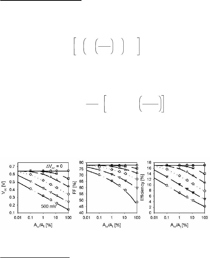
These dependences are plotted in figure 5. For large weak areas, the device voltage is
logarithmic in area and linear in ∆V
oc
. The FF [16] follows the open-circuit voltage. Equation
(2) shows that the total device performance is more sensitive to the voltage deficit in the ìweak
areaî than to the area. For example, 1% of the cell area that is 200 mV weaker than the rest of
the cell reduces the device efficiency by about the same amount as when 12% of the area is 100
mV weaker.
Figure 5. V
oc
dependence on the weak area for several voltage deficits calculated analytically
(lines) and numerically (symbols). The ∆V
oc
step between two lines is 100 mV.
2.c) Finite TCO resistance
When series resistance is finite, J-V curves cannot be calculated analytically without
increasingly more substantial approximation. The impact of the series resistance can, however,
be calculated numerically. When R
s
is small, numerical methods (symbols in figure 5) give very
similar results to the ones obtained by analytical methods (lines in figure 5). TCO resistance
introduces a voltage drop across the TCO and thus isolates the lower-voltage area. Voltage maps
∆V(x,y) = V
s
(x,y) ñV
w
(x,y) are shown in figure 6. V
s
(x,y) is the voltage of a uniform diode as
function of position, and V
w
(x,y) is voltage when 4% of centrally located diodes have V
oc
reduced by 0.4 V.
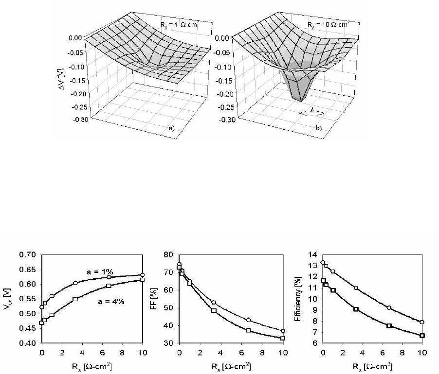
Figure 6. Voltage maps of two solar cells with different R
s
. Applied voltage is 0.5 V, ∆V
oc
= 0.4
V, and
a = 4%.
The effect of different TCO resistances on device performance is shown in figure 7. The
increase in V
oc
due to larger R
s
can be more than 100 mV. The TCO resistance, however,
introduces FF losses that are larger than the voltage gain, and thus the overall effect on the
device efficiency is negative.
Figure 7. Change in nonuniform cell parameters due to TCO resistance. ∆V
oc
= 0.3 V
Since the weak diodes pull down the voltage of the nearest neighbors, it is not surprising
that the distribution of the weak diodes affects the device voltage. Calculated results for a device
with a total 4% weak-diode area show the smallest effect when the diodes are clustered together
towards a corner of the device and the largest when they are scattered throughout the device.
The maximum-power point, and thus the device conversion efficiency, however, is very nearly
independent on the diodesí distribution.
CONCLUSIONS
Submicron CIGS devices are more sensitive to thickness fluctuations than thick ones.
Roughness of 100-nm, for example, should lower the efficiency of a 250-nm cell more than 2%,
but a 1-µm cell less than 0.2%. Although thinner cells have lower lifetimes, they are less
sensitive to lifetime variations then the thicker ones. The impact of the weak diode on the device
performance is linear in its voltage deficit to a first approximation, and the impact of the low-
voltage area is logarithmic. The calculated constant efficiency curves for a high-quality CIGS
cell are shown in figure 8. Areas less than 10% of the total device area with voltage deficits less
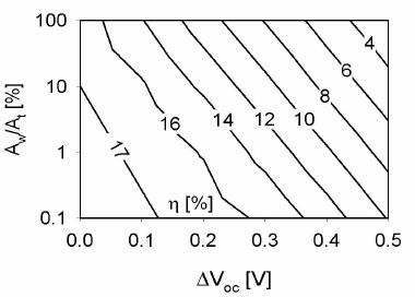
than 100 mV decrease the device efficiency less than 1%. A decrease of 100 mV in V
oc
can
result equally well from a 0.1-eV band-gap fluctuations for any device thickness, a 50%
thickness fluctuation for a 250-nm thick device, or two orders of magnitude decrease in lifetime.
Although the sheet resistance in the TCO can isolate the weak areas and prevent them from
dominating the entire device, it also reduces the fill-factor and the cellsí efficiency.
Figure 8. Efficiency dependence on ∆V
oc
and weak area (baseline efficiency = 17.1%)
ACKNOWLEDGMENTS
This work has been funded by the National Renewable Energy Laboratory. Numerical
simulations are performed with the AMPS-1D software developed at Pennsylvania State
University and with PSpice circuit analysis developed by Cadence Design Systems, Inc.
REFERENCES
1. M. A. Contreras, K. Ramanathan, J. AbuShama, F. Hasoon, D. L. Young, B. Egaas and
R. Noufi, Prog. Photovoltaics 13, 209 (2005).
2. R. N. Bhattacharya, M. A. Contreras, B. Egaas, R. N. Noufi, A. Kanevce and J. R. Sites,
Appl. Phys. Lett. 89, 253503 (2006).
3. T. Negami, S. Nishiwaki, Y. Hashimoto, N. Kohara and T. Wada, in Proc. 2
nd
WCPEC,
(1998) pp. 1181
4. O. Lundberg, M. Bodegard, J. Malmstrom and L. Stolt, Prog. Photovoltaics 11, 77
(2003).
5. K. Ramanathan, R. Noufi, B. To, D.L. Young, R. Bhattacharya, M. A. Contreras, R.G.
Dhere and G. Teeter, in Proc. 4
th
WCPEC, (2006) pp. 380
6. M. Gloeckler and J. R. Sites, J. Appl. Phys. 98, 103703 (2005).
7. V. G. Karpov, A. D. Compaan and D. Shvydka, Phys. Rev. B 69, 045325 (2004).
8. P. O. Grabitz, U. Rau and J. H. Werner, Phys. Status. Solidi A 202, 2920 (2005).
9. P. O. Grabitz, U. Rau and J. H. Werner, Thin Solid Films 487, 14 (2005).
10. J. H. Werner, J. Mattheis and U. Rau, Thin Solid Films 480, 399 (2005).
11. U. Rau, P. O. Grabitz and J. H. Werner, Appl. Phys. Lett. 85, 6010 (2004).
12. V.G. Karpov, A. D. Compaan and D. Shvydka, in Proc. 29
th
IEEE PVSC, (2002) pp. 708
13. V.G. Karpov, R. Harju and G. Dorer, in Proc. 28
th
IEEE PVSC, (2000) pp. 547
14. V. G. Karpov, A. D. Compaan and D. Shvydka, Appl. Phys. Lett. 80, 4256 (2002).
15. I. L. Eisgruber, PhD. Thesis, Colorado State University (1996)
16. M. A. Green: Solar cells, Prentice-Hall, (1982), p. 80.
