Nanometer Metrology of Periodic Structures with Ultrafast Optoacoustics
T.J. Grimsley
1
, G.A. Antonelli
2
, F. Yang
1
, H. J. Maris
1
, A. V. Nurmikko
1,3
1. Department of Physics, Brown University, Providence RI, 02912 USA.
2. External Research & Development, Novellus Systems, Albany, NY 12203 USA.
3. Division of Engineering, Brown University, Providence RI, 02912 USA.
ABSTRACT
We present an optoacoustic method to non-destructively measure the average dimensions
of a periodic array of simple structures with aspect ratios greater than 10:1, which are
inaccessible to AFM techniques. The technique that we describe could be used as the basis of an
inline metrology tool for wafer inspection. The samples examined were test structures with high
precision lithographically defined lines of silicon dioxide deposited on a silicon substrate. The
thickness of the silicon dioxide was around 400 nm, and the gaps between the lines ranged from
100 nm down to smaller than 40 nm. A drop of water was placed on the sample, and an
optoacoustic transducer was placed on top; measurements were taken with a water thickness less
than 1 micron between the optoacoustic transducer and the sample. The water filled the spaces
between the lines due to the hydrophilic nature of the sample surface. Using the picosecond
ultrasonics technique, acoustic pulses are generated in a special optoacoustic transducer,
transmitted through a coupling fluid (water), scattered off of the sample being examined and then
return to the transducer. The returning acoustic signal shows nanometer sensitivity to the height
of the lines and the specific details of their profile.
INTRODUCTION
In the transition to the 22nm node processes and beyond, the semiconductor industry
fabricates structures that are difficult to characterize non-destructively with existing techniques.
In this paper, we examine samples that consist of silicon dioxide lines on a silicon substrate, with
a cap layer of silicon nitride approximately 5 nm thick. The lines were part of a test structure
fabricated by Novellus Systems using precision lithography techniques. The spacing between
the lines was as narrow as 35 nm, and the lines were 405 nm thick. White light scatterometry [1]
can be used to non-destructively characterize these structures at the wafer level; however,
destructive cross-sectional scanning electron microscopy (SEM) remains the industry standard
for extracting geometric information from patterned structures. As dimensions continue to
shrink, these structures will become more difficult to measure with optical techniques;
furthermore, optical techniques require both the dimensional and the optical parameters of the
system to model the measured scattered white light. We present a method for measuring the
dimensions of the nanostructures that is non-destructive, insensitive to its optical properties, and
possible to perform at the wafer level.
The technique of picosecond ultrasonics [2] uses pulses from a mode-locked laser to
generate and detect sound pulses with durations on the order of picoseconds. An ultrashort light
pulse (~150 fs) from the pump beam is absorbed by an optoacoustic transducer. The energy
deposited by the pump pulse generates an elastic stress; as this stress relaxes it launches an
Mater. Res. Soc. Symp. Proc. Vol. 1249 © 2010 Materials Research Society 1249-F10-05
acoustic pulse into the coupling fluid. This pulse then propagates across the coupling fluid
(water) and then reflects and scatters off of the sample. Returning sound that has been reflected
and scattered from the sample modifies the optical reflectivity of the optoacoustic transducer. A
probe pulse that has been delayed in its arrival time monitors changes in reflectivity caused by
the returning sound. The optoacoustic transducer was a Fabry-Perot optical cavity structure just
off resonance at the center wavelength of the laser. Returning sound perturbs the optical
thickness optical cavity, which in turn causes a change in optical reflectivity that is detected by
the probe beam. We report on the application of this technique to metrology problems relevant
to the semiconductor industry [3].
EXPERIMENTAL METHOD
The picosecond ultrasonics technique uses the output of a mode-locked laser to generate
ultra-short acoustic pulses with durations on the order of picoseconds. A schematic of the
experimental configuration is shown in figure 1. The output of a mode-locked laser is split into
two beams, the pump beam and the probe beam. The pump beam is modulated at a frequency of
2 MHz by an electro-optic modulator and is then focused onto the thin aluminum film, and the
absorbed light increases the temperature of the film by approximately 3 K. This change in
temperature generates an elastic strain which relaxes by launching two acoustic pulses. The first
pulse propagates into the glass substrate and contributes to the experimental background, while
the second pulse propagates into the water. The water acts as a coupling liquid for the sound
pulse, which reflects off of the sample being examined and then returns to the transducer
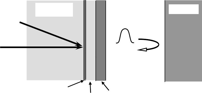
Figure 1. Schematic diagram of the experimental technique employed here. The
transducer structure consists of a stack of films deposited on a glass substrate
(Corning C1737 glass). The pump pulse heats the thin Al film and launches an
acoustic pulse into the water. The pulse then reflects off of the sample and returns to
the transducer structure. When the returning acoustic pulse propagates through the
transducer, it causes a change in the transducers optical reflectivity which is then
detected by the time delayed probe pulse.
PUMP LIGHT
WATER
0.7 mm SiO
2
SUBSTRATE
SOUND
PULSE
7 nm Al
230 nm
SiO
2
100 nm
Al
SAMPLE
PROBE
LIGHT
structure. As the returning sound pulse propagates through the transducer structure, it causes a
change in the optical reflectivity of the structure which is detected by a time delayed probe pulse.
During a measurement the probe pulse time delay is varied from 0 to 4 ns by a retro-reflector
mounted on a mechanical translation stage. The reflected probe light is focused onto a
photodetector and lock-in detection is used to improve the signal to noise ratio.
As the sound pulse propagates through the coupling liquid, the viscosity of the water
serves to decrease the amplitude of the pulse and increase its width. For example, if an acoustic
pulse whose width is initially described by a delta function propagates through 1 micron of
water, its profile will stretch out into a Gaussian shape with a FWHM of 117 nm. In order to
detect the returning acoustic pulses after they have returned from traveling through the coupling
liquid, we used a transducer structure that consists of films of aluminum, silicon dioxide, and
aluminum with thicknesses of 7nm, 246nm, and 100 nm respectively. The transducer structure
acts like a Fabry-Perot optical resonator, whose optical reflectivity as a function of wavelength is
shown in figure 2a. The effective quality factor Q of the transducer is quite low since the
reflectivity of the thin film is approximately 0.5. The calculated variation in the optical
reflectivity of the transducer structure with respect to the thickness of the middle silicon dioxide
film for a wavelength of 800 nm is shown in figure 2b. The thickness of the middle silicon
dioxide layer was chosen to be 230 nm, since this is where the transducer structure is the most
sensitive to perturbations in the optical thickness of the structure. The returning sound will also
perturb the optical properties of the aluminum films as well; this additional perturbation will be
determined by the piezo-optic constants of Al. These have been measured by Jiles and Staines
[4] but are found to vary rapidly for wavelengths around 800 nm. They are also likely to depend
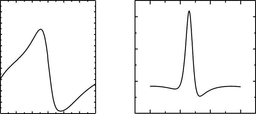
Figure 2. (a) The measured reflectivity of the transducer structure versus
wavelength. (b) The calculated variation of the optical reflectivity of the cavity with
respect to the thickness middle silicon dioxide film, w. The wavelength of the light
is 800 nm and the maximum sensitivity is obtained for a thickness of 230 nm.
100
200
300
400
-0.01
0.00
0.01
0.02
THICKNESS OF SiO
2
(nm)
dR/dw (nm
-
1
)
600
800
1000
0
0.2
0.4
0.6
0.8
1
WAVELENGTH
(nm)
REFLECTIVITY
on the deposition conditions for the aluminum films, and we have made no further effort to
quantify the size of this effect.
DISCUSSION
Experimental results obtained when the sample is a piece of silicon with an unpatterned
surface, and with a water thickness of 280 nm, are shown in figure 3a. The change in reflectivity
that occurs in the first 200 ps is caused by the initial heating of the films in the transducer
structure, which slowly cool down, and the generated strain pulse propagating through the
transducer structure. The fast oscillations in the data, known as Brillouin oscillations, are caused
by alternating constructive and destructive interference between probe light that has reflected
from the cavity and the probe light that has scattered from a sound pulse that propagates into the
silicon dioxide substrate. These oscillations have no effect on the operation of the transducer and
they can be easily subtracted out using a Fourier filter. In figure 3b, we show the first echo from
the silicon surface after subtracting out the slowly decaying background and the fast oscillations.
By varying the thickness of the water and analyzing the Fourier components of the returning
echoes, the sound velocity and attenuation of sound in water for frequencies up to 11 GHz can be
measured, and will be reported elsewhere [5].
Figure 3. (a) The measured change in optical reflectivity taken with a water layer
thickness of 280 nm at a temperature of 23
o
C. (b) The first acoustic echo in the data
of (a) with the thermal background and the Brillouin oscillations subtracted.
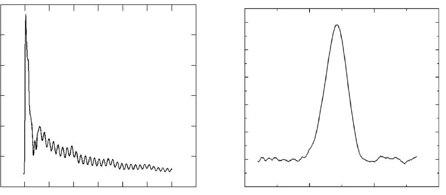
A cross sectional SEM of sample A is shown in figure 4a. The average depth of the
trenches between the silicon dioxide lines is measured to be 405 nm. The repeat distance of the
pattern in sample A is 240 nm, and the width of the trench half way down is 45 nm. The lines
cover an area of about 0.1 by 0.5 mm, which is much larger than the spot sizes of the pump and
the probe beam. The probe spot has a diameter of about 20 microns, which means that
approximately 80 trenches are being measured at once. The first echo at a time delay of 1700
ps is from the portion of the acoustic pulse that is reflected from the tops of the silicon dioxide
0 500 1000
1500
TIME DELAY (ps)
REFLECTIVITY CHANGE (a.u.)
200 400 600 800
TIME DELAY (ps)
REFLECTIVITY CHANGE (a.u.)
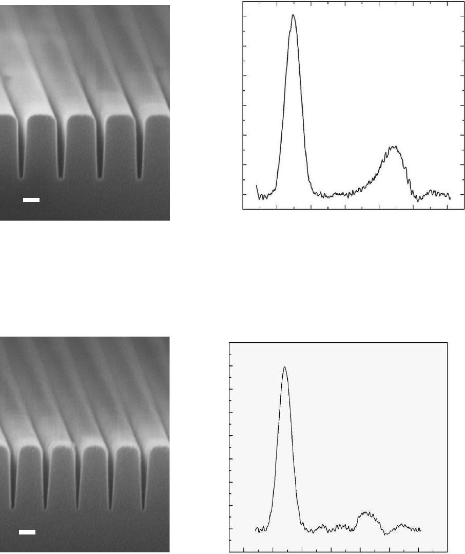
Figure 4. (a) SEM cross section of sample A (scale bar 100nm long). The height of
the silicon dioxide lines is measured to be 405 nm, and the width of the channel
halfway down the channel is 45 nm. (b) Acoustic echoes from the top and bottom of
the channels in sample A at a temperature of 23
o
C. The data was processed in the
same manner as in figure 3b.
Figure 5. (a) SEM cross section of sample B (scale bar 100 nm long). The height of
the silicon dioxide lines is measured to be 405 nm, and the width of the channel
halfway down the channel is 35 nm. (b) Acoustic echoes from the top and bottom of
the channels in sample B at a temperature of 23
o
C. The data was processed in the
same manner as in figure 3b.
1400 1600 1800
2000
2200 2400 2600
TIME (ps)
0.2
0.6
0.8
1.0
0.4
1.2
REFLECTIVITY CHANGE (x10
-
6
)
0.0
1400 1600 1800 2000 2200 2400 2600
TIME (ps)
1.2
0.4
1.6
REFLECTIVITY CHANGE (X10
-
6
)
1200
0.8
0.0
lines, and the second echo that arrives at a time delay of 2280 ps is from sound that has
penetrated into the channels between the lines and reflected off of the bottom. The difference in
the arrival times for the echoes in figure 4b is 580 ± 2 ps. The time required for sound to travel
through 810 nm of water, a distance equal to a round trip through the channel, is 544 ps; the
effect of the interaction between the channel walls and the viscous fluid is to slow and attenuate
the sound pulse.
A cross sectional SEM of sample B is shown in figure 5a. The average width of the
channels in sample B is 35 nm halfway down the channel. The acoustic echoes from sample B
are shown in figure 5b. Narrowing the channels by 10 nm significantly reduces the magnitude of
the echo from the bottom. The difference in the arrival times of the echoes from the top and the
bottom is 560 ± 3 ps; the sound in the channel is propagating slower than sound in bulk water,
but is going slightly faster than the sound when it propagates in the channels in sample A. This
is surprising and is presumed to be a consequence of the different profiles of the trenches in the
two samples. In future work, we plan on studying experimentally and by computer simulation a
series of samples to explore the effect of the trench width and profile on the shape, amplitude,
and time of arrival of the acoustic echoes. At this point we emphasize the shape of the acoustic
echo from the bottom of the channel was quite sensitive to the width of the channel.
CONCLUSIONS
In this paper we have presented a non-destructive optical method for measuring the
average heights of silicon dioxide lines. The structures that we examined had dimensions and an
aspect ratio that would be difficult to characterize using other techniques such as AFM. In future
work we plan to explore further the relationship between the surface profile of the sample and
the features of the acoustic signature. We are also in the process of developing a version of this
apparatus that will use an acoustic lens to focus sound pulses on individual nanostructures.
This work was supported in part by the Department of Energy through grant DE-SC0001988.
REFERENCES
1. P. de Groot, X. C. de Lega, J. Liesener, and M. Darwin, Phys. Rev. Lett. 16, 3970 (2008).
2. C. Thomsen, H. T. Grahn, H. J. Maris, and J. Tauc, Phys. Rev. B 34, 4129 (1986).
3. A preliminary account of this work, examining structures with aspect ratios smaller than those
presented here, has appeared. See, T.J. Grimsley, C.H. Dang, Q. Zhang, S. Che, F. Yang, G. A.
Antonelli, A.V. Nurmikko, H.J. Maris, "Picosecond Ultrasonic Microscopy of Semiconductor
Nanostructures", in Proceedings of the International Symposium on Laser Ultrasonics (July
2008).
4. D. Jiles and M. P. Staines, Sol. State Comm. 47, 37 (1983).
5. “Picosecond Ultrasonics Experiments with Water and its Application to the Measurement of
Nanostructures”, (F. Yang, T. J. Grimsley, S. Che, G. A. Antonelli, H. J. Maris, and A. V.
Nurmikko), to appear in J. Appl. Phys.
