Materials Strategies for Advanced NanoTechnology
Kyung Choi
Nanotechnology, Bell Labs., Lucent Technologies, 600-700 Mountain Ave, Murray Hill,
NJ, 07974
We demonstrate ‘functional microfabrications’ by synthesizing new functional polymers.
Photopatternable silicon elastomers have been designed for high fidelity, functional
microfabrication purposes to integrate dynamic devices. ‘Elastic photopatterns’ generated
by using molecularly modified silicon elastomers have been demonstrated since
functional microfabrications are beneficial to develop elastic devices with high
resolutions for our diverse applications.
INTRODUCTION
Materials scientists and chemists have sought for the development of new materials and
novel microfabrication techniques to fabricate high performance devices.
1-7
We explored
novel materials strategies to bring new advances in nanotechnology by developing
functional polymers since nanotechnology is a part of chemical domain. We present
novel chemistry here to modify conventional silicon elastomers thus to extend current
nanotechnology to an advanced level for our diverse needs.
There are many promising technologies in nanotechnology such as soft lithography,
nanofabrications, functional pattern fabrications, and microfluidic technology. However,
commercial materials, which were developed for other purposes, often show limitations
for our specific purposes in nanotechnology. For this reason, we described here novel
chemical approaches to overcome the limitations in conventional materials thus to
achieve new advances in nanotechnology by developing new materials.
Soft lithography has been widely used to transfer small patterns from the masters to
substrates for integrating electronic patterns. Silicon elastomers are used for stamping or
microprinting purposes in pattern transfers. Sylgard 184 commercially produced from
Dow Corning, has been used in current soft lithography. However, those commercial
silicon rubbers often result in mechanical failures such as collapses, mergences, and
disconnections of features; especially, there are a lot of limitations for fabricating patterns
at the nano-scale regimes using Sylgard 184. Since it is beneficial for us to modify
chemical structures of commercial silicon rubbers, we introduced photopatternable
silicon rubbers in this study to satisfy our multiple demands. To overcome the limitations,
we designed and synthesized a new version of stamp materials.
Silicon rubbers are based on poly(dimethyl)siloxane network. Its highly elastic property
has been used for stamping and microfabrications.
Mater. Res. Soc. Symp. Proc. Vol. 1004 © 2007 Materials Research Society 1004-P06-08
Highly stretchable property of silicon elastomers is originated from the Si-O-Si structure
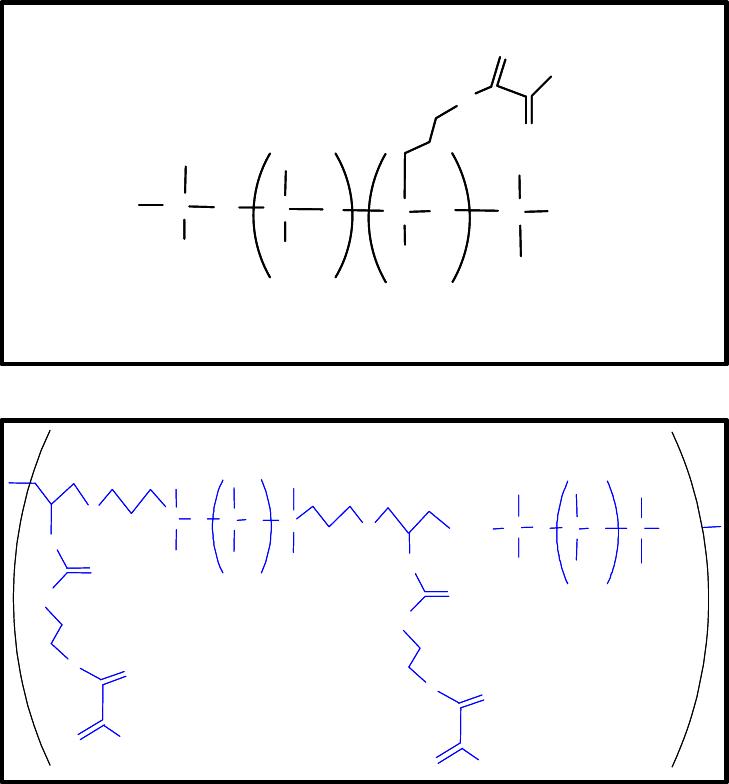
combined with cross-linked structure. Figure 1 illustrates a comparison of molecular
structures between conventional and designed photocurable PDMS prepolymers.
Figure 1. Chemical structures of (top) commercial photocurable and (bottom)
synthesized photocurable silicon rubbers.
Top of Figure 1 illustrates a chemical structure of a commercially available, photocurable
PDMS prepolymer; it is available from Gelest Inc. The bottom one shows a chemical
structure of synthesized, photocurable PDMS prepolymer. As shown in their structures,
both structures have photocurable methacrylate cross-linkers. However, the commercially
available silicon elastomer shown in Figure 1, revealed significant mechanical failures
during pattern transfers due to its low mechanical strength.
O
O
CH
3
Si
O
CH
3
CH
3
Si
CH
3
CH
3
CH
3
Si
CH
3
CH
3
O
Si
CH
3
O
e
f
Catalog #: Gelest, RMS-033
O
O
Si
O
CH
3
CH
3
Si
CH
3
CH
3
OSi
CH
3
CH
3
O
O
HN
O
CH
3
O(R) Si
O
CH
3
CH
3
Si
CH
3
CH
3
O
Si
CH
3
CH
3
(R)O
k
m
n
O
O
O
HN
O
CH
3
O
O
O
CH
3
Si
O
CH
3
CH
3
Si
CH
3
CH
3
CH
3
Si
CH
3
CH
3
O
Si
CH
3
O
e
f
Catalog #: Gelest, RMS-033
O
O
Si
O
CH
3
CH
3
Si
CH
3
CH
3
OSi
CH
3
CH
3
O
O
HN
O
CH
3
O(R) Si
O
CH
3
CH
3
Si
CH
3
CH
3
O
Si
CH
3
CH
3
(R)O
k
m
n
O
O
O
HN
O
CH
3
O

We thus modified the chemical structure of commercial silicon elastomers to achieve
enhanced mechanical stiffness since mechanical rigidity of stamp materials is
significantly related to the lithographic and patterning performances. As shown in Figure
1, the synthesized PDMS prepolymers have longer and stiffer cross-linkers compared to
that of the commercial one. The designed cross-linkers have produced a good mechanical
strength of synthesized PDMS during patterning transfers.
RESULTS AND DISCUSSION
We designed a new version of photocurable PDMS prepolymers by inserting novel
photocurable cross-linkers onto PDMS prepolymer networks. In order to improve
physical toughness of PDMS stamps, we provided new silicon elastomers with cross-
linkers containing urethane groups; because, urethane groups bring high mechanical
toughness to minimize mechanical collapses during lithographic and pattern transferring
tasks. The designed photocurable silicon prepolymer is denoted as hυ-PDMS
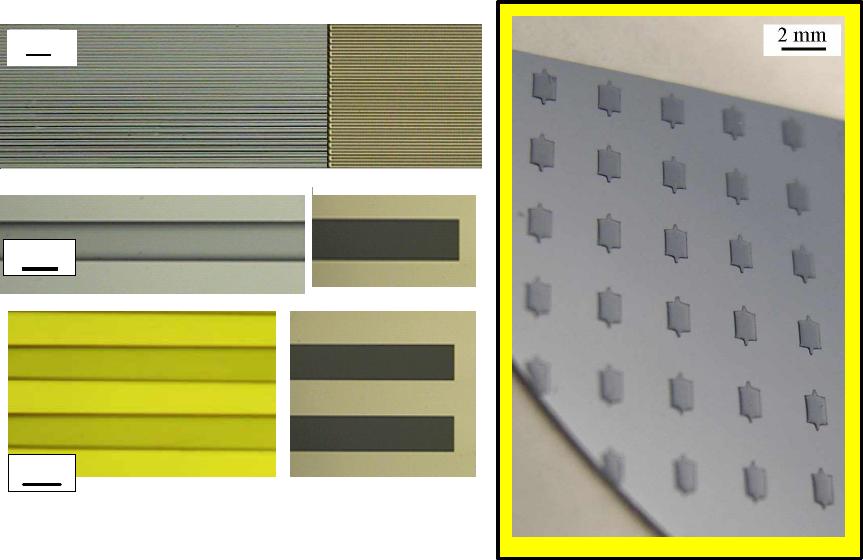
prepolymer. Figure 2 shows SEM images of the original master (submicron-scale features
of 300 nm line-width and 600 nm thickness) and the corresponding hυ-PDMS mold.
Figure 2. SEM images of the master and corresponding patterns transferred onto hυ-
PDMS mold.
Master
Mold (hυ-PDMS)
Master
Mold (hυ-PDMS)
Master
Mold (hυ-PDMS)
For elastic microfabrications of hυ-PDMS prepolymer, the hυ-PDMS prepolymer was
spin-coated on silicon wafers. Subsequently, original masks were placed on the hυ-
PDMS prepolymer layer, followed by UV exposure using a UVP Blak-Ray lamp at 365
nm for 1 min. It was then soaked into an ethanol bath for development. Microscopic
images of elastic microfabrications are shown in Figure 3.
Figure 3 shows microscopic images of various micro-features generated on silicon wafers
using hυ-PDMS prepolymer. Those patterns shown in Figure 3 are based on elastic
silicon rubbers in line-width size ranges of <100 µm, which weren’t easy to fabricate
using the commercial photocurable PDMS system.
As shown in Figure 3, performance of elastic photopatterning fabrications shows high
resolution with those micro-features. Modified PDMS prepolymers show the
improvements in functional microfabrications due to its adjustable mechanical stiffness.
We also carried out the microfabrications of elastic photopatterns in smaller sizes to
explore of pattern transfers using features in the smaller scale with 5µm-width striped
patterns. The result shows in the right frame of Figure 3.
As you can see in those images, hυ-PDMS prepolymers have produced ‘elastic
photopatterns’ with ~ 5 µm accuracy, which wasn’t be successful from commercial
photocurable PDMS prepolymers.
Figure 3. Elastic photopatterns generated on silicon wafer using hυ-PDMS prepolymer.
100 µm
Masters
Elastic photopatterns
100
µ
m100
µ
m
30
µ
m30
µ
m
100 µm
Masters
Elastic photopatterns
100
µ
m100
µ
m100
µ
m100
µ
m
30
µ
m30
µ
m30
µ
m30
µ
m30
µ
m
In conclusion, we demonstrate here a novel chemical strategy to synthesize stiffer,
photocurable PDMS prepolymers with adjustable mechanical strengths, that brings our
desired properties in materials for high fidelity soft lithography and functional
microfabrications in the submicron -scale regime for our diverse applications. We present
a specific advantage of the stiffer PDMS stamps, such as high resolution ‘elastic
photopatternability’. This result encourages us to develop new materials for
nanotechnology purposes.
REFERENCES
1. (a) E. Kim, Y. N. Xia, and G. M. Whitesides, J. Am. Chem. Soc. 118, 5722 (1996).
(b) Y. N. Xia, J. A. Rogers, K. E. Paul, and G. M. Whitesides, Chem. Rev. 99, 1823
(1999).
2. (a) K. M. Choi and J. A. Rogers, J. Am. Chem. Soc. 125, 4060 (2003).
(b) K. M. Choi, J. Phys. Chem. 109, 21525 (2005).
3. P. G. Conrad, P. T. Nishmura, D. Aherne, B. J. Schwartz, D. Wu, N. Fang, X. Zhang,
J. Roberts, K. J. Shea, Adv. Mater. 11, 5274 (2003).
4. T. Thorsen, S. J. Maerkl and S. R. Quake, Science 298, 580 (2002).
5. X. Duan, C. Niu, V. Sahi, J. Chen, J. W. Parce, S. Empedocles, J. L. Goldman,
Nature 425, 274 (2003).
6. T. Wu, Y. Mei, J. Cabral, C. Xu, K. L. Beers, J. Am. Chem. Soc. 126, 9880 (2004).
7. J. Kobayashi, Y. Mori, K. Okamoto, R. Akiyama, M. Ueno, T. Kitamori, S.
Kobayashi, Science 304, 1305 (2004).
