A Band Structure Phase Diagram Calculation of 2D BiSb Films
Ming Y. Tang
1
and Mildred S. Dresselhaus
1,2
1
Department of Electrical Engineering and Computer Science,
Massachusetts Institute of Technology, Cambridge,
MA 02139, U.S.A.
2
Department of Physics, Massachusetts Institute of Technology,
Cambridge, MA 02139, U.S.A.
ABSTRACT
Ever since the birth of thermoelectrics, it has been well known that semiconductors
(materials with a relative small bandgap) give the best thermoelectric performance. From
quantum mechanics, it is also well known that low dimension quantum confinement leads to
changes in the band alignment of a material. Thus, a semimetallic material can be made
semiconducting by using low dimensionality quantum confinement effects. BiSb alloys have
been of particular interest for thermoelectric application in the temperature range of 70K to
100K. In bulk form, BiSb alloys can either be a semimetal or a semiconductor, depending on the
alloy composition. Moreover, semimetallic BiSb alloys can be made semiconducting by using
the low dimensionality quantum confinement concept. With these two previous concepts in
mind, it is valuable to further explore the dependence of the band alignment for different alloy
concentrations and different confinement conditions for BiSb alloys.
Following the study of the effect of the Sb concentration and of the wire diameter on the
semimetallic or semiconducting phase of BiSb alloy nanowires [1], we now examine the
corresponding effect of the Sb concentration and the film thickness on the properties of BiSb
alloy films. A band structure phase diagram is calculated, giving the details on the dependence
of the relative band edge position on the film thickness and the Sb concentration. This phase
diagram gives a first hand guideline for choosing the film thickness and the Sb concentration to
better improve the thermoelectric performance of BiSb alloy films.
INTRODUCTION
In the 1990s, using low dimensional physics concepts, Hicks and Dresselhaus predicted that
a dramatic enhancement in thermoelectric performance was possible through the use of quantum
wells and quantum wires [2, 3]. In the late 1990s, Chen also predicted that an enhancement in
ZT could result from the significant reduction in the thermal conductivity in a low dimensional
system [4]. At the same time, nano-fabrication technology rapidly improved during the last
decade. With advances in technology and in new low dimensional concepts, increases in the
thermoelectric figure of merit (
2
/( )
eph
ZT S T
σ
κκ
=+ where
σ
is the electrical conductivity, S is
the Seebeck coefficient,
e
κ
and
ph
κ
are respectively the electrical and lattice thermal
conductivity, and T is the temperature) have been demonstrated [5].
Refrigeration is one of the major applications for thermoelectric materials. The advantage
of thermoelectric refrigeration is the absence of moving compressor units as is done using
conventional refrigerators. Thermoelectrics not only decrease the noise level and the weight of
the refrigerator, they also increase the refrigerator life cycle.
BiSb alloys have been of particular interest for thermoelectric refrigeration in the
Mater. Res. Soc. Symp. Proc. Vol. 886 © 2006 Materials Research Society 0886-F04-05.1

temperature range of 70K to 100K. It has always been important for the research community to
have theoretical guidelines before working with thermoelectric materials for the desired
applications, because of the large number of variables that need to be considered in laboratory
demonstrations. Following the study of the dependence of the semimetallic or semiconducting
phase of BiSb alloys nanowires on Sb concentration and on wire diameter [1], this paper now
examines the corresponding effect of the Sb concentration and the film thickness on the
properties of BiSb alloy films. The results of this study give guidelines for choosing the film
thickness and the Sb concentration to improve the thermoelectric performance of BiSb alloy
films.
BACKGROUND
Bismuth (Bi)
Figure 1. Crystal structure (left) and Brillouin zone (right) of Bismuth. The dark gray near-
center Bi atom is displaced along the trigonal axis such that the distance between that Bi atom
and the bottom dark Bi atom is different than the distance between the near-center dark gray Bi
atom and the top dot-shaded Bi atom.
Bismuth (Bi) is a group V element and is a semimetal in bulk form. Bi is the most
diamagnetic of all metals, and its thermal conductivity is the 2
nd
lowest among all metals, next to
that of mercury. Bi has a high electrical resistance and has the highest Hall effect of any metal
[6]. The crystal structure of Bi is rhombohedral with two atoms per unit cell. Its unit cell can be
described as a FCC unit cell stretched along the trigonal direction with a small displacement of
the near-center Bi atom from the central location (see Figure 1). Due to these two distortions,
the degeneracy at the L <111> points is lifted, and the T points [111,
111] are structurally
distinct from the 6 structurally equivalent L points [
111 , 111, 111, 111, 111, and 111 ] in the
distorted rhombohedral structure that describes Bi, Sb, and BiSb alloys (see Figure 1). In
crystalline bulk Bi, there is an overlap of 38meV between the conduction band at the L points
and the valence band at the T points. Bi is an anisotropic material with a ratio of greater than
100 for the maximum and minimum sized wave vectors of its Fermi surface.
z Trigonal (3)
x Binary (1)
y Bisectrix (2)
α
0886-F04-05.2

Bismuth-Antimony (BiSb)
Figure 2. Band structure of Bi
1-x
Sb
x
alloy as a function of Sb concentration x [7]. The Brillouin
zone is shown as an inset, indicating the location of one of the L points, one of the T points, and
3 of the 6 H points.
Bismuth and Antimony are both group V elements and semimetals in bulk form. They are
completely miscible with each other, are isoelectronic, and have very similar chemical
properties. However, due to the larger structural distortions in Sb, the valence band of Sb is
located at the H points instead of the T points (see Figure 2). The introduction of Sb into Bi
changes the band structure of Bi and gives rise to a transition between a semimetal and a
semiconductor (see Figure 2). The extra control on the system parameters by the addition of Sb
provides a promising approach to achieve a desirable band structure for the desired
thermoelectric applications.
RESULTS
Bi thin film calculation
To understand the behavior of the Bi
1-x
Sb
x
system under investigation, the Schrödinger
equation for this system needs to be solved for the energy eigenvalues and wavefunctions.
However, from the effective mass theorem [8], knowing the envelope wave function is sufficient
to describe many properties of the system. Thus, it is sufficient within the effective mass
approximation to solve for the envelope function of the system without solving for the exact
wavefunctions.
For each electronic energy band (conduction or valence), we start with the effective mass
model
2
(,,) (,,)
2
x
yz E xyz
αψ ψ
−∇••∇ =
=
(1)
where the inverse effective mass tensor is given by
SM
SC
SM
Bismuth Antimony
H
T
L
0886-F04-05.3

11 12 13
1
12 22 23
13 23 33
M
ααα
αααα
ααα
−
⎛⎞
⎜⎟
≡=
⎜⎟
⎜⎟
⎝⎠
,
(2)
and when we carry out the dot products in Equation (1) , we obtain the result
222 2 2 2
11 22 33 12 13 23
222 2
2
222
E
xyz xyxzyz
ψψψ ψ ψ ψ
α
αα α α α ψ
∂∂∂ ∂ ∂ ∂
+++ + + =−
∂∂∂ ∂∂∂∂∂∂=
.
(3)
If we let the trigonal axis be the film growth direction, the envelope function could then be
written as
(,,) () [ ]
y
x
z
ik y
ik x
ik z
xyz uze e e
ψ
= ,
(4)
and the equation can be solved for the wavefunctions and the eigenenergies to obtain:
22
22 2
22
13 23 13 23
11 22 12
33 33 33
22
33
2
2
{( ) ( ) (2 )}
22 2
2
xy xy
Ek k kku
u
z
αα αα
αα α
αα α
α
+−+ +−+ +− +
∂
=−
∂
== =
=
.
(5)
Once the eigenenergies and wavefunctions for each subband for the film are obtained by solving
Equation (5), the properties of the thin film system can be studied. We are interested in both the
solutions for general k vectors and for the solution at the bandedge. We note that in the case of a
thin film solution for the band edge energy (k
x
=k
y
=0), this solution is very similar to the particle-
in-a-box solution. Putting the eigenvalue solution for the band edge energy in the form of
particle-in-a-box solution results in an equation of the following form for each subband
222
*
0
2
()
2
n
Ek k
L
π
α
==
K
=
,
(6)
where
= is Planck’s constant, L = film thickness,
α
* = inverse effective mass in the film growth
direction for the band under investigation, and n=1,2,3,… is the subband index. For our case
where the film growth direction is along the trigonal axis, the inverse effective mass is
α
*=
α
33
.
Applying Equation (6) to the Bi thin film system with the growth direction along the trigonal
axis for each subband at a temperature range of around 77K, it is found that the semimetal-
semiconductor transition occurs at a critical film thickness (d
c
) of about 65nm (see Figure 3).
Previous publications have estimated a d
c
of 100nm [9] and 13nm [10] for the same system
under investigation. This discrepancy is mainly due to the different temperature range in interest
and the lack of consideration for the anisotropic nature of Bi from previous works.
Fermi level and transport properties are other parameters of interest for our system. Due to
the non-parabolic nature of the L conduction bands and the different transport effective masses
between the L electrons and the H or T holes, the Fermi level will change depending on the film
thickness and Sb concentration. The Fermi level calculation will be presented in detail along
with the transport properties evaluation in our upcoming publication.
0886-F04-05.4

Figure 3. Bi thin film calculation of the energy for the valence and conduction band extrema as
a function of film thickness for the film growth direction along the trigonal axis. The
semimetallic-semiconducting transition occurs at a film thickness of around 65nm.
BiSb thin film calculation
Combining the thin film calculation (from the previous subsection) with the band structure
of the BiSb alloy (see Figure 2), a BiSb 2D film phase diagram is generated (see Figure 4).
The BiSb 2D film phase diagram possesses similar physics when compared with the
previous work for the nanowire system [1]. Starting from the pure Bi region, the increase in Sb
concentration decreases the overlap between the T points and L points, resulting in an increase in
film thickness (a decrease in the amount of quantum confinement) needed for the occurrence of
the semimetal-semiconductor transition. A similar behavior is observed when we start from the
Sb-rich regions. Two especially interesting phenomenon for the phase diagram worth noting are
that: (1) the system is gapless at each of the semimetal-semiconductor transition boundaries and
(2) the valence band T points, valence band H points, and conduction and valence bands L points
of the Bi thin film system all have the same energy at the middle point of the phase diagram.
Thus, at regions near the point of high band degeneracy, this system not only has the potential of
being a good candidate for low temperature thermoelectric applications, it may also be used as an
extremely sensitive meV detector due to its high density of states (DOS) near its band extrema.
Due to the anisotropic nature of Bi and the different confinement direction between this
work (the trigonal direction) and previous work (the bisectrix and binary directions) [1], there is
no clear direct comparison between these works of the length scales for the semimetal-
semiconductor transition. However, in general, for an isotropic or a close-to-isotropic system,
the length scales for the observation of quantum effects should increases as the dimension of
confinement increases. In the case of thin films, quantum confinement is in the film direction,
while for the nanowires, quantum confinement occurs in the two directions normal to the axis of
the quantum wire.
Decreasing film thickness
Semimetal
Semiconductor
0886-F04-05.5
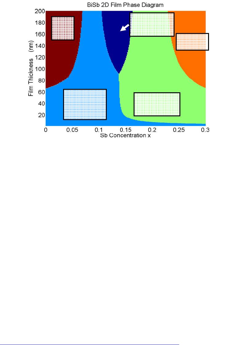
Figure 4. A BiSb 2D film Phase Diagram. The semimetallic and semiconducting regions are
noted. For each region, the location of the valence band extrema and the conduction band
extrema are indicated by the notation valence
öconduction. And for the semiconducting
phases, the indirect and direct gap phases are distinguished.
SUMMARY
Using the quantum confinement principle and the addition of Sb, a 2D Phase Diagram for
BiSb film has been computed. This 2D Phase Diagram gives guidelines for designing desired
BiSb thin films for thermoelectric applications.
ACKNOWLEDGEMENTS
The authors gratefully thank valuable discussions with Dr. Gene Dresselhaus, Dr. Oded
Rabin, and Dr. Yu-Ming Lin, and support from NSF/NIRT (CTS-0506830) for this work.
REFERENCES
1. O. Rabin, Y.-M. Lin, and M.S. Dresselhaus, Appli. Phys. Lett., 2001.
79(1): p. 81-83.
2. L.D. Hicks and M.S. Dresselhaus, Phys. Rev. B, 1993.
47: p. 12727-12731.
3. L.D. Hicks and M.S. Dresselhaus, Phys. Rev. B, 1993.
47: p. 16631-16634.
4. G. Chen, Phys. Rev. B, 1998.
57: p. 14958-14973.
5. R. Venkatasubramanian, et al., Nature, 2001.
413: p. 597-602.
6. http://www.pmel.org/HandBook/PeriodicTable/periodic.htm
.
7. B. Lenoir, et al., J. Phys. Chem. Solids, 1998.
59(1): p. 129-134.
8. T.P. Orlando, S.D. Senturia, and P.L. Hagelstein, Physics for Solid State Applications. p.
Chapter 7.
9. V.N. Lutskii, Sov. Phys. - JETP. Lett., 1965.
2: p. 245-248.
10. S. Takaoka and K. Murase, J. Phys. Soc. Jpn., 1985.
54(6): p. 2250-2256.
direct
semiconductor
L->L
indirect
semiconducto
r
T->L
indirect
semiconductor
H->L
semimetal
L->H
semi-
metal
L->T
0886-F04-05.6
