Investigation of Retention Properties for YMnO
3
Based
Metal/Ferroelectric/Insulator/Semiconductor Capacitors
T. Yoshimura, D. Ito, H. Sakata, N. Shigemitsu, K. Haratake, A. Ashida and N. Fujimura,
Department of Applied Materials Science, Graduate School of Engineering,
Osaka Prefecture University, Sakai, Osaka, Japan
ABSTRACT
The memory retention properties of Pt/YMnO
3
/Y
2
O
3
/Si capacitors were investigated for the
application of ferroelectric gate transistors. The epitaxially grown Pt/YMnO
3
/Y
2
O
3
/Si capacitors
showed ferroelectric type hysteresis loop on the capacitance-voltage properties. Although the
retention time of the as-deposited capacitors was ~10
3
s, it was prolonged up to 10
4
s when the
leakage current density was reduced from 4×10
-8
A/cm
2
to 2×10
-9
A/cm
2
by the annealing under
N
2
ambience. To reveal the relationship between the retention time and leakage current, the
leakage current mechanism was investigated comparing several conduction mechanisms. It was
found that the dominant leakage mechanisms at high and low electric fields were Poole-Frenkel
emission from the Y
2
O
3
layer and ohmic conduction, respectively. This result indicates that the
leakage current was limited by the Y
2
O
3
layer at high electric field and was mainly dominated by
the amount of defects in the YMnO
3
layer at low electric field. From the pseudo isothermal
capacitance transient spectroscopy (ICTS), it was determined that the trap density was in an order
of 10
15
cm
-3
. Since the variation of the leakage current by annealing was observed only in the low
electric field region, it is suggested that the retention properties of the Pt/YMnO
3
/Y
2
O
3
/Si
capacitors was influenced by the amount of defects in the YMnO
3
layer.
INTRODUCTION
Ferroelectric gate field-effect transistors (FETs) have been investigated for the applications to
nonvolatile memory devices due to the nondestructive read operation and the advantages of
decreasing memory cell size[1,2]. Because of the difficulty to obtain the excellent ferroelectric-
semiconductor interface, ferroelectric gate FETs with a metal-ferroelectric(-metal)-insulator-
semiconductor (MF(M)IS) structure have been widely studied[3-5]. We have investigated YMnO
3
films for MFIS type ferroelectric gate FET, because YMnO
3
has suitable properties for this
application such as small spontaneous polarization and low permittivity[6,7]. We have succeeded
in fabricating YMnO
3
epitaxial films with a remanent of 3.4 µC/cm
2
on (111)Pt/sapphire
substrates and epitaxially grown (0001)YMnO
3
/(111)Y
2
O
3
/(111)Si capacitors with ferroelectric
type C-V hysteresis loop[8,9]. In this study, the degradation mechanisms of the memory retention
for Pt/YMnO
3
/Y
2
O
3
/Si capacitors are discussed.
EXPERIMENTAL PROCEDURE
An n-type Si(111) single crystal wafer with 1 Ωcm resistivity was used as a substrate. The
substrate was chemically cleaned using hot solutions (80 ºC) of NH
4
OH:H
2
O
2
:H
2
O (=1:1:5) and
HCl:H
2
O
2
:H
2
O (=1:1:6), and 1% HF acid. After cleaning, Y
2
O
3
epitaxial films with a thickness of
20 nm and YMnO
3
films with a thickness of 400 nm were deposited on the Si substrate by a pulsed
Mat. Res. Soc. Symp. Proc. Vol. 786 © 2004 Materials Research Society E9.7.1/C9.7.1
laser deposition (PLD) method (ULVAC, ULP-1000) with an eximer laser (Lambda Physic)
operated at a wavelength of 248 nm. Details of the deposition of the YMnO
3
/Y
2
O
3
/Si capacitors
were described elsewhere[8]. An rf magnetron sputtering deposition system was used for
depositing top Pt electrode within the area of 900 µm
2
through a shadow mask. Dielectric and
ferroelectric measurements were conducted using MFIS configuration at room temperature. The
capacitance was measured using an LCR meter (HP 4284A) with small ac amplitude of 25 mV
from 20 Hz to 1 MHz. The leakage current was measured using a pico-ampere meter (HP 4140B)
from 0 V to 10 V at a step of 0.2V and a step delay time of 10s. The voltage was applied to the top
electrode. The retention property of MFIS capacitors was characterized by the change in the
capacitance at flat band voltage. The retention time was defined when the difference of the
capacitance after charged by the positive and negative electric field was reduced to 50%.
RESULTS AND DISCUSSION
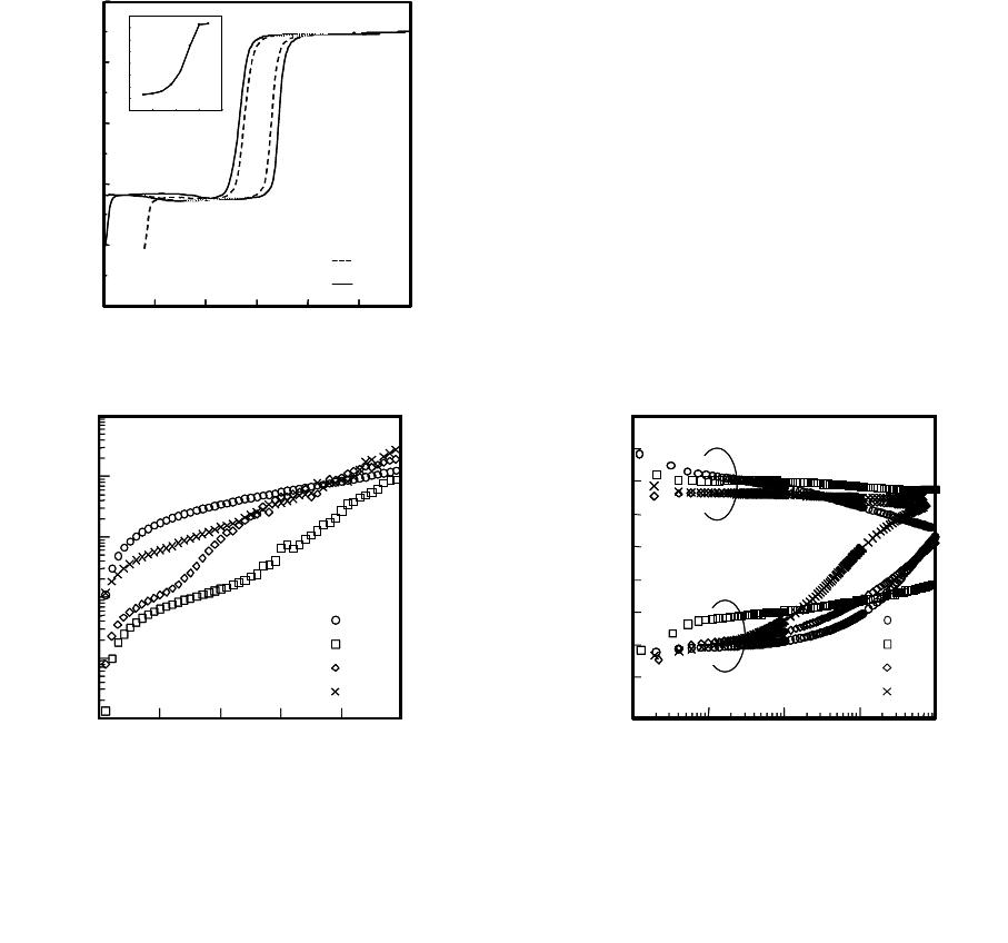
Figure 1 shows a C-V property of an epitaxially grown YMnO
3
/Y
2
O
3
/Si capacitor. The C-V
Figure 2. I-V properties of the epitaxial
Pt/YMnO
3
/Y
2
O
3
/Si capacitor. (a) as-depo. (b) N2
annealed (c) O
2
annealed (3 min) (d) O
2
anneale
d
(6 min)
Figure 3. Retention properties of the epitaxial
Pt/YMnO
3
/Y
2
O
3
/Si capacitor. (a) as-depo. (b) N
2
annealed (c) O
2
annealed (3 min) (d) O
2
anneale
d
(6 min)
Capacitance (pF)
10
0
10
1
10
2
10
3
10
4
Time (s)
5
7
9
11
13
15
17
19
21
23
V
po l
=+15 V
t
pol
=100 ms
(b)
(a)
(c)
(d)
V
po l
=-15 V
Leakage current density (A/cm
2
)
10
-11
10
-9
10
-7
Applied Voltage (V)
02 684
10
-6
10
-8
10
-10
10
(b)
(a)
(c)
(d)
(b)
(a)
(c)
(d)
Capacitance (pF)
25
10
15
20
0
0510-5-10 15-15
Applied Voltage (V)
11V
15V
7V
5
Applied Voltage (V)
Memory window (V)
Capacitance (pF)
25
10
15
20
0
0510-5-10 15-15
Applied Voltage (V)
11V
15V
7V
5
Applied Voltage (V)
Memory window (V)
Figure 1. C-V properties of the epitxial
Pt/YMnO
3
/Y
2
O
3
/Si capacitor. The inset is the
width of the memory window as a function of
applied voltage.
E9.7.2/C9.7.2
property shows the ferroelectric type hysteresis with a memory window saturated at ±13 V. Figure
2(a) shows the I-V properties of the capacitor. No bias voltage was applied. The leakage current
density of the as-deposited capacitor at 3 V was below 10
-7
A/cm
2
. As have been reported, one
reason for the increased leakage is due to excess oxygen[10]. Therefore, annealing in nitrogen for
10 min was attempted. As shown in Fig. 2(b), the leakage current density in the low electric field
region could be decreased to 2×10
-9
A/cm
2
by the annealing. In addition, the leakage current
density of the capacitor annealed in nitrogen increased after annealing in oxygen ambient (Fig.
2(c) and (d)). This result agreed well with that the origin of the leakage current of YMnO
3
films is
excess oxygen.
Figure 3 shows the retention properties of the YMnO
3
/Y
2
O
3
/Si capacitors which have various
leakage current densities changed by annealing. Although the leakage current was changed, the
saturation of the memory window was observed in the C-V property. The retention time of the
as-deposited capacitor was about 10
3
s (Fig. 3(a)). As can be seen, the capacitor with lower leakage
current shows longer retention time. By annealing in nitrogen ambience, the retention time was
prolonged up to 10
4
s (Fig. 3(b)). As shown in Fig. 2, the change in the leakage current density was
obvious in the low-voltage region. In contrast, it was small in the high-voltage region. In order to
investigate the relationship between the retention property and the leakage current in detail, the
I-V properties were analyzed comparing several leakage current mechanisms[11]. Since the
YMnO
3
and Y
2
O
3
layers have different dielectric properties, the electric field applied to the each
layer must be different. To estimate the each electric field, the dielectric constants of YMnO
3
and
Y
2
O
3
layers were assumed as 75 and 10 based on the experimental results. The dielectric constant
of YMnO
3
was calculated using not the capacitance measured by the LCR meter but the
polarization hysteresis loop, because the actual induced charge at ferroelectric film surface can not
be calculated by the linear component of the dielectric constant. The ratio of the electric field
applied to YMnO
3
and Y
2
O
3
layers was calculated by that the MFIS capacitor was considered as
two capacitors in series. Using the thicknesses of YMnO
3
and Y
2
O
3
layers (400 and 20 nm,
respectively), the ratio of 73:27 was obtained.
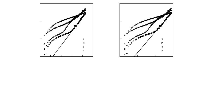
First, the I-V properties of the capacitor were analyzed using Schottky and Poole-Frenkel
(P-F) emission models. Figures 4(i) and (ii) show the Schottky plots of the I-V properties using the
electric field of the YMnO
3
and Y
2
O
3
layers, respectively. Linear relationships were obtained at
high electric field. The dielectric constant was calculated from Fig. 4(i) and (ii) using the equation
of Schottky emission J
sh
,
Figure 4 Schottky plots of the I-V properties using the electric field of (i) YMnO
3
and (ii) Y
2
O
3
layers.
(a) as-depo. (b) N
2
annealed (c) O
2
annealed (3 min) (d) O
2
annealed (6 min)
0245
E
1/2
((MV/m)
1/2
)
ln (J/T
2
)
-16
-20
-24
-28
31 04 12
E
1/2
((MV/m)
1/2
)
ln (J/T
2
)
-16
-20
-24
-28
8
(b)
(a)
(c)
(d)
(b)
(a)
(c)
(d)
(i) (ii)
E9.7.3/C9.7.3
E
kT
qq
kT
q
TJ
i
B
sh
0
2
4/
~)/ln(
επε
+
Φ
− , Eq. (1)
where
k is Boltzmann constant, T is temperature, q is electron charge,
ε
i
is dielectric constant, Φ
B
is the barrier height. The dielectric constants calculated from Fig. 4(i) and (ii) are 0.2 and 1.6,
respectively. These are obviously too low compared with the dielectric constants of YMnO
3
and
Y
2
O
3
. This suggests that Schottky emission is not the dominant leakage mechanism. Figures 5(i)
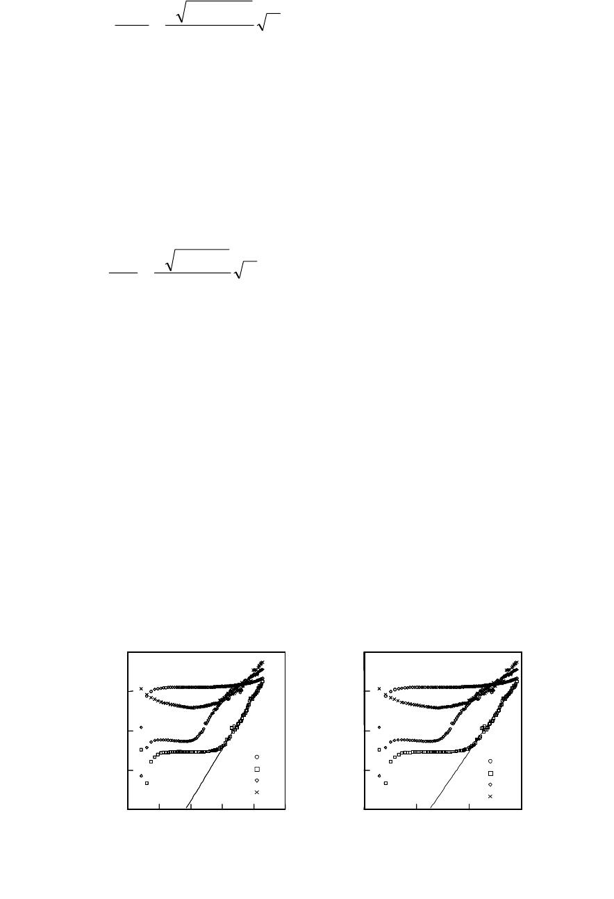
and (ii) show the P-F plots of the I-V properties using the electric fields of the YMnO
3
and Y
2
O
3
layers, respectively. In both plots, although the inclines of the plots at low electric field are
negative, linear relations with positive incline were obtained in the high electric field region. From
the equation of P-F emission,
J
PF
,
E
kT
qq
kT
qW
EJ
i
t
PF
0
/
~)/ln(
επε
+− , Eq(2)
where
Wt is barrier height,
ε
i
can be calculated by the incline of the plot. At the high electric field
region, the dielectric constants calculated using the electric fields of YMnO
3
and Y
2
O
3
are 1.2 and
9.1, respectively. The later is reasonable value for the dielectric constant of Y
2
O
3
. Therefore, this
indicates that the dominant leakage mechanism of the Pt/YMnO
3
/Y
2
O
3
/Si capacitor at the high
electric field region is P-F emission from the Y
2
O
3
layer. It should be noted that the effect of the
annealing on the leakage current is small at the high electric field region. It is suggested that the
annealing affects the electrical properties of YMnO
3
.
Figure 6 shows logJ vs lodV plots of the I-V properties. Since the slope of the plot in low
electric field region is nearly 1, the leakage current at low electric field can be explained by ohmic
conduction[11]. The effect of the annealing on the leakage current is clearly observed in the low
electric field region. From the result of the retention properties shown in Fig. 3, it is suggest that
the ohmic conductance at low voltage is greatly related to the retention property and that making
the ohmic conductance at low voltage small should be effective to prolong the memory retention
time.
Since it is known that ohmic conductance at low voltage is caused by the charge trapping to
defects in the film, we attempted to evaluate the defect density that influenced the memory
Figure 5 P-F plots of the I-V properties using the electric field of (i) YMnO
3
and (ii) Y
2
O
3
layers.
(a) as-depo. (b) N
2
annealed (c) O
2
annealed (3 min) (d) O
2
annealed (6 min)
-22
-24
-26
-28
ln (J/E)
-30
04812
ln (J/E)
E
1/2
((MV/m)
1/2
)
-24
-26
-28
-30
-32
0245
E
1/2
((MV/m)
1/2
)
31
(b)
(a)
(c)
(d)
(b)
(a)
(c)
(d)
(i) (ii)
E9.7.4/C9.7.4
retention. The retention property can be considered to be the capacitance-retention time (C-t)
property. Therefore, we attempted to obtain the “pseudo ICTS spectrum” from the retention
properties. In case of normal ICTS spectrum, the change of capacitance is measured for short time
under the inversion condition of MIS capacitor to detect the emission from traps in the
semiconductor. In contrast, pseudo ICTS spectrum, which is obtained from the retention
properties of MFIS capacitor, is from the change of capacitance for long time (>>1s) under no bias
condition. In addition, the inversion condition of MFIS capacitor is maintained by not bias voltage
but the remanent polarization of the ferroelectric layer. Therefore, pseudo ICTS spectrum should
reflect the status of traps in the ferroelectric layer, because the change of capacitance is the
relationship between the remanent polarization and traps. ICTS signal was derived using the
following formula,
()
()
[]
()
[]
ττεε
ttVVNqdtdCttS
biTs
−⋅−=⋅= exp2
0
2
, (Eq. 3)
where
S(t) is ICTS signal. E
a
, N
T
and τ are activation energy, the trap density and the time constant
of the carrier emission, respectively. Therefore, these parameters of the Pt/YMnO
3
/Y
2
O
3
/Si
capacitor can be obtained from pseudo ICTS signal.
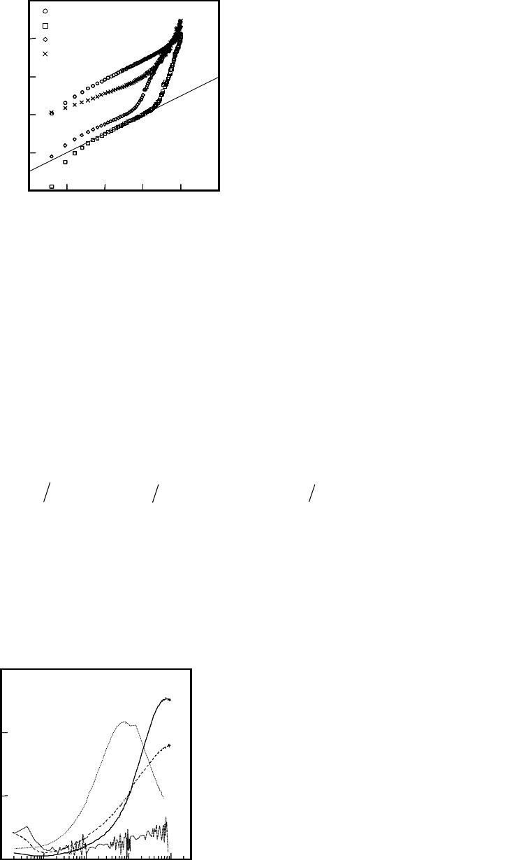
Figure 7 shows the pseudo ICTS spectra of the Pt/YMnO
3
/Y
2
O
3
/Si capacitor. Except the
capacitor annealed in N
2
ambient, a peak was observed in the spectra. It seems that the trap density
of the N
2
annealed capacitor is too low to detect in this measurement time. The trap density, N
T
,
Time (s)
1 10 100 1000 10000
S(t)
(c)
(a)
(b)
(d)
Figure 7 Defect density calculated from
Pseudo ICTS spectra
Figure 6 The logJ vs lodV plots of the I-V
p
roperties. (a) as-depo. (b) N
2
annealed (c)
O
2
annealed (3 min) (d) O
2
annealed (6 min)
-1 1
Log (V)
Log (J)
-6
-8
-10
0
Slope=1
(b)
(a)
(c)
(d)
E9.7.5/C9.7.5
was calculated from the intensity and τ of the peak of the pseudo ICTS spectra. The trap densities
of (a) as-deposited, (c) O
2
annealed (3 min) and (d) O
2
annealed (6 min) were 8.8×10
15
, 6.3×10
15
and 7.6×10
15
cm
-3
, respectively. Thus, the trap density of the Pt/YMnO
3
/Y
2
O
3
/Si capacitor
decreases as decreasing the leakage current at low electric field. From these results, the retention
degradation mechanism of the Pt/YMnO
3
/Y
2
O
3
/Si capacitor can be explained as follows. Traps in
YMnO
3
layer affect the leakage current of the capacitor at low electric field. During the retention,
the remanent polarization of YMnO
3
was neutralized by the leakage current which is induced by
the depolarization field in the YMnO
3
layer. The retention time is prolonged with decreasing the
trap density of the YMnO
3
layer, because the leakage current at low electric field and the amount
of the trapped charge are decreased.
CONCLUSIONS
The relationship between the leakage current and memory retention properties of
Pt/YMnO
3
/Y
2
O
3
/Si capacitors was investigated. It was found that the leakage current of the
capacitors could be decreased by the annealing in nitrogen and that the retention time was
prolonged from 10
3
to 10
4
s. From the analysis of the leakage current, it was revealed that at high
electric field, Poole-Frenkel emission from Y
2
O
3
layer was the dominant leakage mechanism. On
the other hand, the dominant leakage current mechanism at low electric field, which has strong
relationship with the retention time, was ohmic conduction. Although further investigations such
as temperature and time dependences are needed to eliminate the
transient current effects etc., it is
suggested that the reduction of defects is important to improve the retention property.
ACKNOWLEDGMENTS
This work was supported by a Grant-in-Aid for Scientific Research (B), No. 08555078,
from the Ministry of Education, Science, Sports, and Culture of Japan, a Grant-in-Aid for
Scientific Research, No. 13875009, a Grant-in-Aid Exploratory Research, No. 13875009,
Grant-in-Aid for Scientific Research (S), No. 14102021 from the Japan Society for the Promotion
of Science, and THE MURATA SCIENCE FOUNDATION.
REFERENCES
1. J.L. Moll and Y. Tarui, IEEE trans. Elect. Dev., ED-10, 338 (1963)
2. H. Ishiwara, Jpn. J. Appl. Phys., 32, 442 (1993)
3. I. Sakai, E. Tokumitu and H. Ishiwara, Jpn. J. Appl. Phys., 35, 4987 (1996)
4. Y. Oishi, Y. Matsumuro and M Okuyama, Jpn. J. Appl. Phys., 36, 5896 (1997)
5. Y. Fujisaki, T. Kijima, and H. Ishiwara, Appl. Phys. Lett., 78, 1285 (2001)
6. N. Fujimura, T. Ishida, T. Yoshimura, and T. Ito, Appl. Phys. Lett., 69, 1011 (1996)
7. T. Yoshimura, N. Fujimura, D. Ito and T. Ito, J. Appl. Phys., 87, 3444 (2000)
8. D. Ito, N. Fujimura, T. Yoshimura, and T. Ito, Journal of Applied Physics, 93, 5563 (2003)
9. D. Ito, N. Fujimura, T. Yoshimura, and T. Ito, Journal of Applied Physics, 94, 4036 (2003)
10. K. Kakuno, D. Ito, N. Fujimura, T. Ito, J. Crys. Growth, 237-239, 487 (2002)
11. D. R. Lamb, Electrical conduction mechanisms in thin insulating films, (Methuen and co ltd,
London, 1967)
E9.7.6/C9.7.6
