
http://journals.cambridge.org Downloaded: 22 Mar 2015 IP address: 138.251.14.35
Epitaxial growth and interfaces of high-quality InN films grown on
nitrided sapphire substrates
Fangliang Gao, Yunfang Guan, and Jingling Li
Department of Electronic Materials, State Key Laboratory of Luminescent Materials and Devices,
South China University of Technology, Guangzhou 510640, China
Junning Gao
State Key Laboratory of Solidification Processing, Northwestern Polytechnical University, Xi’an 710072, China
Junqiu Guo and Guoqiang Li
a)
Department of Electronic Materials, State Key Laboratory of Luminescent Materials and Devices,
South China University of Technology, Guangzhou 510640, China
(Received 16 November 2012; accepted 26 February 2013)
InN films have been grown on sapphire substrates nitrided by N plasma with different durations
by radio-frequency plasma assisted molecular beam epitaxy (RF-MBE). In-depth investigation
reveals that AlN is generated on a sapphire surface during the nitridation, and 60 min nitridation
helps in the formation of an ordered and flat AlN interlayer between the substrate and the InN
film, which improves the surface migration of In atoms on the substrate, and consequently helps
in obtaining a single-crystalline c-plane InN film of high quality with 1.0 10
19
cm
3
carrier density
and 1350 cm
2
/(Vs) carrier mobility. Too short nitridation duration will result in a polycrystalline InN
film, and too long nitridation duration will damage the surface quality of the newly generated AlN
interlayer which consequently deteriorates the InN film quality. Control of the AlN interlayer quality
plays a critical role in the growth of a high-quality InN epitaxial film on the sapphire substrate.
I. INTRODUCTION
Indium nitride (InN) has attracted considerable attention
recently because of its outstanding electrical and optical
properties. Among III-nitride semiconductors, InN has
the lowest electron effective mass, the highest peak-drift
velocity and the highest peak overshoot velocity, which
are beneficial for high-electron-mobility transistors
(HEMTs).
1,2
Moreover, InN has a direct band gap of
;0.7 eV which enables the III-nitride s emiconductors
to cover the wave length from deep ultraviolet (AlN,
Eg 5 6.2 eV) to near infrared (InN, Eg 5 0.7 eV).
3,4
InN has
shown great potential in the fields of terahertz emitters,
5–8
light-emitting
9
and photovoltaic applications,
10
etc.
In 1972, Hovel and Cuomo
11
grew InN thin films on sap-
phire by using radio-frequency sputtering for the first time.
With the development of thin film growth technology,
researchers have obtained InN thin films using various
techniques, such as hydride vapor phase epitaxy (HVPE),
12
metal organic chemical vapor deposition (MOCVD),
13
radio frequency plasma assisted molecular-beam epitaxy
(RF-MBE),
14
pulsed laser deposition (PLD),
15,16
etc.
However, it is still difficult to obtain high-quality InN due
to its high equilibrium vapor pressure, low dissociation
temperature of nitrogen and the lack of suitable substrates
for InN.
17
To date, sapphire is the most common substrate to grow
III-nitride semiconductors. However, InN shares an up to
25% mismatch with sapphire in terms of lattice parameter
which results in polycrystalline InN films when directly
growing InN on sapphire. A large number of grain bound-
aries existing in polycrystalline InN films slow down trans-
portation of carriers. As a result, the performance of devices
is deteriorated. Consequently, single-crystalline InN films
are highly desired. If sapphire substrates are nitrided
before the growth of InN films, a thin nitrided layer might
be formed on the sapphire surface. This nitrided layer,
i.e., AlN interlayer, can act as a buffer between sapphire
and I nN. As pointed out, InN shares a lattice mismatch
of 25% and 13.9% with sapphire and AlN, respectively.
Therefore, the generation of an AlN interlayer on the
surface of a sapphire substrate dramatically decreases the
lattice mismatch between InN and sapphire. Meanwhile,
it should be noted that In atoms have strong adhesion on
sapphire substrates, which results in low lateral migration
and accumulation of In atoms on the sapphire surface,
leading to a rough surface of th e as-grown InN film.
The formation of an AlN interlayer on the other hand
prohibits the accumulation of In atoms on the sapphire
surface, so as to provide a smooth surface and a good
template for the succeeding InN epitaxial growth, which
plays an important role in improving the film quality of
a)
Address all correspondence to this author.
e-mail: [email protected]
DOI: 10.1557/jmr.2013.67
J. Mater. Res., Vol. 28, No. 9, May 14, 2013 Ó Materials Research Society 2013 1239

http://journals.cambridge.org Downloaded: 22 Mar 2015 IP address: 138.251.14.35
the as-grown InN film on sapphire. In this paper, we focus
on the influence of sapphire nitridation on the formation of
a nitrided interlayer, as well as its impact on the as-grown
InN film quality, and consequently propose an optimal
nitridation condition and its corresponding interlayer state
for high-quality InN films grown on sapphire substrates.
II. EXPER IMENTAL
InN films were grown by RF-MBE on (0001) sapphire
substrates. High purity indium (7N) and nitrogen gas (7N)
were used as the sources, respectively. Sapphire substrates
were degreased by organic solvents, etched in a hot so-
lution of H
2
SO
4
and H
3
PO
4
(H
2
SO
4
:H
3
PO
4
5 3:1) at
160 °C for 30 min, rinsed with deionized water, and finally
dried by 7N nitrogen before being put into the MBE load-
lock chamber with pressure 1 10
7
Torr. The substrates
were then transferred into the high vacuum MBE growth
chamber at pressure 1.0 10
10
Torr, and thermally
cleaned at 800 °C for 30 min to remove residual surface
contaminations. Before InN growth, the nitridation of
sapphire was carried out at 550 °C with a nitrogen flow
rate of 1 sccm and a RF plasma power of 240 W.
Subsequently, a low-temperature InN buffer layer was
grown at 350 °C for 5 min with a nitrogen flow rate of
2 sccm and a RF plasma power of 400 W. In the end, a
high-temperature InN layer was grown at 550 °C for
60 min with a nitrogen flow rate of 2 sccm and a RF plasma
power of 240 W. A quartz crystal microbalance (QCM)
was used to monitor the deposition rate during the growth.
It reveals that the thicknesses for the low- and the high-
temperature InN layers are 10 and 200 nm, respectively.
The as-grown InN films were evaluated by x-ray diffraction
(XRD, with Cu K
a1
as an x-ray source) for crystallinity by
Bruker D8 Discover. Cross-sectional high resolution trans-
mission electron microscopy (HRTEM) was carried out to
study the interfaces between the substrates and InN films.
The HRTEM samples were put into a JEOL 3000F field
emission gun TEM (Tokyo, Japan) working at a voltage of
300 kV, which gives a point to point resolution of 0.17 nm.
Electron energy loss spectroscopy (EELS) collections were
carried out under scanning TEM mode, where a spot
formed by a 0.6 nm diameter electron beam was used to
scan across the interface with an interval of 1 nm between
two spots. Scanning electron microscopy (SEM) was then
carried out to evaluate the microstructure of InN films by
FEI Nova NanoSEM 430 (Hillsboro, OR). Hall effect
measurements were also performed at room temperature
to obtain carrier characteristics with a 3000 Gauss magnet.
III. RESULTS AND DISCUSSION
Figure 1 shows the XRD patterns for InN films grown
on (0001) sapphire nitrided with different durations of 20,
30, 50, 60, and 120 min, respectively. Peaks located at
31.02 and 64.66° are from hexagonal InN (0002) and (0004)
planes, those at 33.0 and 69.22° are from InN (10-11) and
(20-22) planes, and the one at 41.6° is from sapphire (0006)
plane. Apparently, InN films grown on sapphire substrates
with nitridation durations of 20, 30, and 50 min are poly-
crystalline with two growth directions of ,0001. (c axis)
and ,10-11., while InN films grown on sapphire sub-
strates with nitridation durations of 60 and 120 min a re
single-crystalline with c axis as the growth direction.
This indicates that the nitridation duration of the sapphire
substrate plays a critical role in determining the crystal-
line form and the growth direction of as-grown InN films.
Too short nitridation duration of sapphire substrates leads
to polycrystalline InN films, while a nitridation duration
of longer than 60 min helps to obtain single-crystalline
InN films on sapphire substrates.
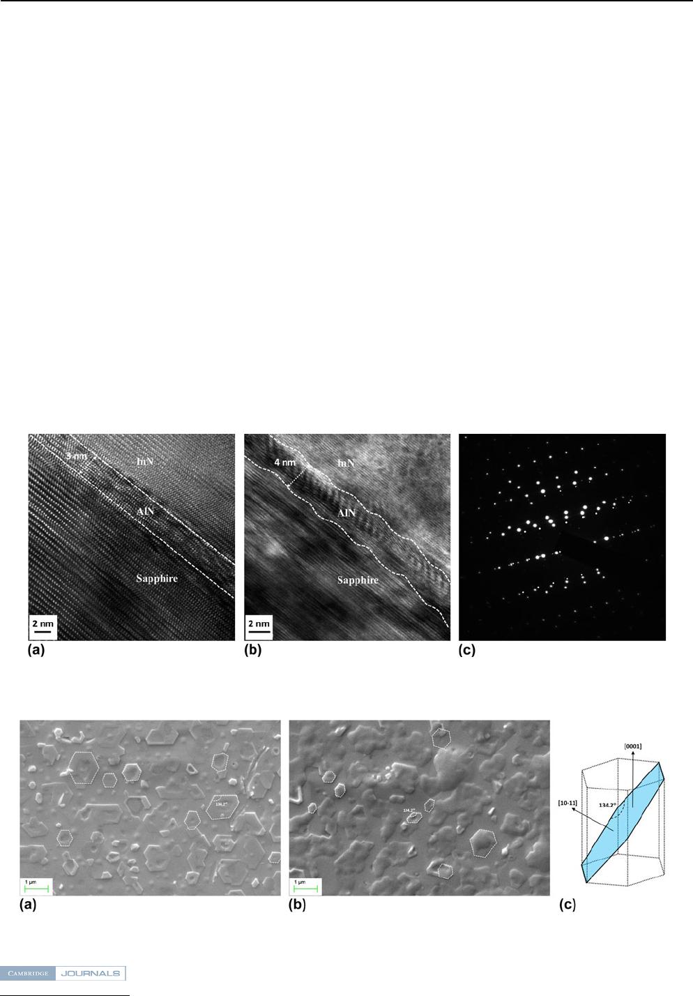
To better understand this finding, HRTEM is carried
out to study the interface between the sapphire substrate
and the InN epitaxial film. Figure 2(a) is the HRTEM
image for an InN sample with 60 min nitridation. One can
clearly notice a continuous interlayer with the thickness of
;3 nm between the sapphire substrate and the InN epi-
taxial film. This continuous interlayer is very flat and
ordered, as illustrated by the two parallel dotted lines in
Fig. 2(a). The concentration of this interlayer has also been
characterized by EELS attached to this TEM. It reveals
that only Al and N are contained in this interlayer, and no
trace of O is detected. EELS measurement further reveals
that the atomic ratio between Al and N is 1, or equally,
AlN. It suggests that the following reaction take places
when sapphire substrates are nitrided by N plasma at high
temperature,
Al
2
O
3
þNðplamsaÞ!AlN þ N
x
O
y
: ð1Þ
The newly generated N
x
O
y
is in the gaseous state and
will be exhausted by the MBE pumping system, leaving a
FIG. 1. XRD patterns of the InN films grown on (0001) sapphire
substrates with various nitridation durations.
F. Gao et al.: Epitaxial growth and interfaces of high-quality InN films grown on nitrided sapphire substrates
J. Mater. Res., Vol. 28, No. 9, May 14, 20131240
http://journals.cambridge.org Downloaded: 22 Mar 2015 IP address: 138.251.14.35
fresh AlN surface on the sapphire substrate. Selected area
electron diffraction around this interface by TEM is given
in Fig. 2(c). Careful investigation lets us to spot three
groups of diffractions, from sapphire, AlN, and InN, re-
spectively. It once again confirms the existence of the AlN
interlayer.
Interestingly, further increase in nitridation duration will
lead to a poorer-quality interlayer, as shown in Fig. 2(b),
the cross-sectional HRTEM image of an InN sample with
120 min nitridation. The thickness of the interlayer with
120 min nitridation is ;4 nm, which is only slightly thicker,
other than 2 times thicker considering the nitridation dura-
tion, than that after 60 min nitridation. It suggests that after
a continuous AlN interlayer is formed following 60 min
nitridation, it becomes much more difficult for N plasma
to diffuse and penetrate the interlayer and react with the
internal sapphire. More important information we get from
Fig. 2(b) is that the interlayer with 120 min nitridation
becomes very wavy and rough, and also much more stressed
and disordered when compared with the straight and smooth
interlayer surface with 60 min nitridation. This wavy and
rough AlN interlayer undoubtably has a negative impact on
the surface migration of In atoms on the substrate surface,
which deteriorates the quality of the subsequently grown
InN film that has been verified by our Hall effect mea-
surement of the samples as discussed later. TEM findings
suggest that too long exposure to the highly energetic N
plasma will damage the surface of the interlayer and hence
the as-grown InN film quality, which is consistent with our
SEM observation.
The surface morphology of the as-grown InN films is
characterized by SEM. Figures 3(a) and 3(b) show those
with nitridation duration of 20 and 30 min, respectively.
We note that both samples share a similarly rough mor-
phology. Apart from those coalesced or overlapped grains,
we can also clearly notice two types of grains with dif-
ferent shapes, as representatively stand out in the images.
Bear in mind that XRD measurement has revealed that
both the films will have two growth directions, i.e., ,00 01.
and ,10-11.. As a reference, we schematically illustrate
these two growth directions and their corresponding planes
in the InN’s wurtzite structure, Fig. 3(c), only to find out the
shapes of the two types of grains match perfectly with the
{0001} and {10-11} planes, respectively. We can then
FIG. 2. (a) Cross-sectional HRTEM images around the interface between the sapphire substrate and the InN film with (a) 60 min and (b) 120 min
nitridations, and (c) the corresponding selected area electron diffraction pattern of (a), where 3 groups of patterns could be spotted.
FIG. 3. SEM images of InN films grown on sapphire substrates nitrided for (a) 20 min and (b) 30 min, respectively, and (c) the schematic illustration
of a InN’s wurtzite structure as well as its two growth directions of ,0001. and ,10-11..
F. Gao et al.: Epitaxial growth and interfaces of high-quality InN films grown on nitrided sapphire substrates
J. Mater. Res., Vol. 28, No. 9, May 14, 2013 1241
http://journals.cambridge.org Downloaded: 22 Mar 2015 IP address: 138.251.14.35
deduce that those of regular hexagonal shapes are from InN
grown along the ,0001. direction, and those of irregular
hexagonal shapes are from InN grown along the ,10-11.
direction. The sizes of two types of grains are within the
same range, from ;0.5 to 1.0 lm, and the proportion of
the two types of grains are almost the same. A further in-
crease in nitridation duration of the sapphire substrates up
to 50 min will not change the surface morphologies of InN
films, which has been confirmed by SEM observation.
Obviously, under this polycrystalline growth condition with
nitridation duration no longer than 50 min, the two types of
grains share the same growth opportunity and no one will
prevail over the other.
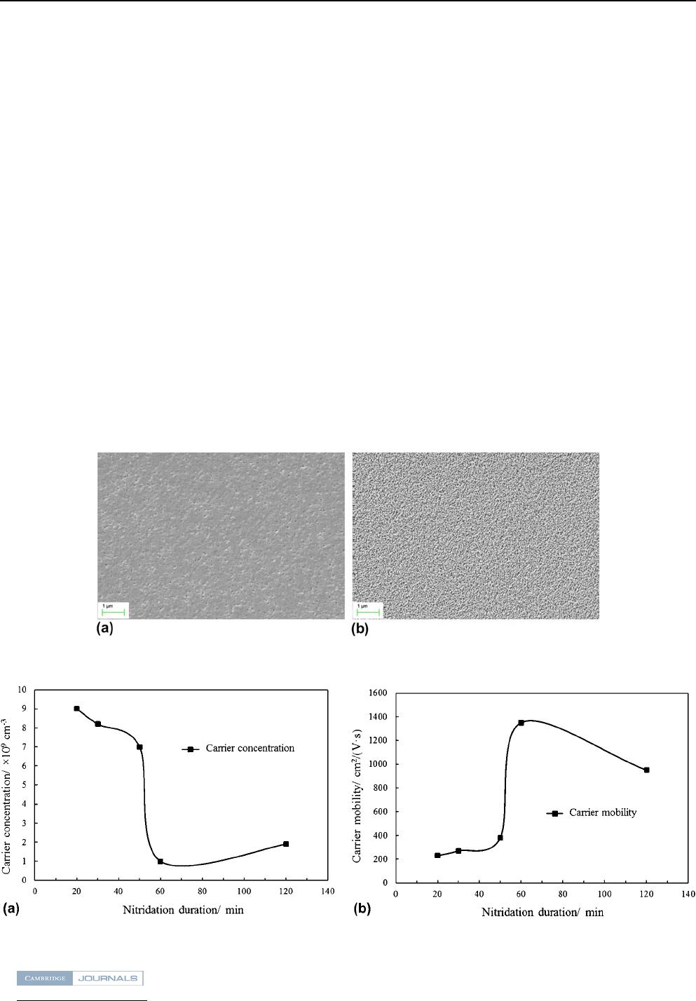
Figure 4(a) shows the SEM image of an InN film grown
on a sapphire substrate nitrided for 60 min. Different from
InN films with less than 50 min nitridation, this film con-
tains grains only of ,0001. growth direction. These grains
coalesce to each other very well, leading to a much flatter
surface than those polycrystalline films. Figure 4(b) shows
the SEM image of an InN film grown on a sapphire sub-
strate nitrided for 120 min. Surprisingly, this film exhibits
much smaller uncoalesced grains and a much rougher sur-
face when compared with the InN film nitrided for 60 min,
although both films are single-crystalline. Obviously, a too
long nitridation duration actually damages the film quality
of the as-grown InN film.
Room-temperature Hall effect measurement has been
carried out with a 3000 Gauss magnet to characterize the
carrier transportation properties of the as-grown InN films.
For this purpose, samples were cut into 10 10 mm
2
and
In foil was pressed on to form the van der Pauw configura-
tion with Ohmic contacts. As we know, InN has a very large
electron affinity.
18–20
Therefore, it is not surprising that
all of our as-grown undo ped InN films exhibit n-type
conductivity, due to the pinning of the Fermi level above
the conduction band edge. Figure 5(a) shows the carrier
concentration for the as-grown samples as a function of
nitridation duration. We find that polycrystalline InN
films have much higher carrier concentration than single-
crystalline InN, which we attribute to the defects in poly-
crystalline films due to the poor surface migration of In
atoms on sapphire substrates.
21
Among polycrystalline
InN samples with nitridation duration no longer than
50 min, the increment in nitridation duration slightly de-
creases the carrier concentration, implying some more AlN
islands formed on sapphire substrates which enhances the
surface migration of In atoms and hence the film quality.
A steep drop in carrier concentration takes place at 60 min
FIG. 4. SEM images of InN films grown on sapphire substrates nitrided for (a) 60 min and (b) 120 min.
FIG. 5. Room-temperature Hall effect measurement of as-grown InN films with various nitridation durations. (a) Carrier concentration, and
(b) carrier mobility.
F. Gao et al.: Epitaxial growth and interfaces of high-quality InN films grown on nitrided sapphire substrates
J. Mater. Res., Vol. 28, No. 9, May 14, 20131242

http://journals.cambridge.org Downloaded: 22 Mar 2015 IP address: 138.251.14.35
nitridation, from 5.5 10
19
to 1.0 10
19
cm
3
, which in-
dicates a very high quality InN film. This is because of the
formation of the continuous AlN interlayer, and conse-
quently the dramatically improved surface migration of In
atoms on the substrate. However, a further increment in
nitridation duration will raise the carrier concentration,
Fig. 5(a), from 1.0 10
19
to 1.9 10
19
cm
3
, indicating a
worsen InN film quality. As discussed above, we attribute
this to the roughened surface of the AlN interlayer due to
too long bombarding by highly energetic N plasma, which
decreases In atom surface migration.
Figure 5(b) shows the carrier mobility for the as-grown
samples as a function of nitridation duration. The as-grown
InN films grown with nitridation durations of 20, 30, 50, 60,
and 120 min have a carrier mobility of 230, 270, 380, 1350,
and 950 cm
2
/(Vs), respectively. Similar to what happens
to the carrier concentration, polycrystalline InN samples
with nitridation duration no longer than 50 min show very
poor carrier mobility of less than 400 cm
2
/(Vs), and single-
crystalline InN samples with 60 min nitridation show very
high film quality with carrier mobility up to 1350 cm
2
/(Vs).
Likewise, further increases in nitridation duration up to
120 min will damage the AlN interlayer quality, which
appears as a diminishing carrier mobility of 950 cm
2
/(Vs).
The results from Hall effect measurement once again con-
firm the importance of an optimal nitridation duration of
sapphire substrates to the as-grown InN film quality. In other
words, 60 min nitridation brings up with a smooth and or-
dered AlN interlayer on top of sapphire which improves the
surface migration of In atoms in InN films, and consequently
enhances carrier properties.
It is not hard to understand that there is an optimal
value for the nitridation duration. Too short nitridation
duration will be not enough to form a continuous AlN layer
on the sapphire surface, and a proportion of sapphire sur-
face is still exposed to In atoms during the growth where
In atoms will unavoidably accumulate. Under such a circum-
stance, as-grown InN films will be polycrystalline with a
rough surface. On the contrary, if nitridation duration is
long enough (up to 60 min), a continuous AlN interlayer
can fully cover the sapphire surface. In atoms obtain much
better migration ability on AlN. Moreover, InN shares much
smaller in-plane lattice mismatch with AlN. The epitaxial
growth condition along c axis for the InN film has therefore
been achieved. Accordingly, a single-crystalline InN film is
grown. If a nitridation duration longer than 60 min is applied
to sapphire substrates, the newly formed continuous AlN
interlayer will be enduring too long bombarding by the
highly energetic N plasma which damages the surface of the
interlayer, resulting in a decrease in InN film quality.
IV. CONCLUSIONS
InN films have been grown on sapphire substrates nitrided
with different durations by RF-MBE. It is found that
nitridation duration of the sapphire substrates determines
the as-grown film quality. Nitridation duration of no longer
than 50 min will end up with a polycrystalline InN film
with two growth directions of ,0001. and ,10-11.,
while nitridation duration of 60 min will bring up with
a single-crystalline c -plane InN film of high quality with
1.0 10
19
cm
3
carrier density and 1350 cm
2
/(Vs) carrier
mobility. However, a further increment in nitridation
duration will worsen the as-grown quality though it is still
single-crystalline.
EELS analysis on the interlayer between the InN film and
the nitrided sapphire substrate by cross-sectional HRTEM
reveal that AlN is generated on the sapphire surface during
the nitridation by N plasma, and 60 min nitridation leads
to a continuously straight and smooth AlN interlayer of
;3 nm which enormously enhances the surface migration
of In atoms on the substrate, resulting in a high-quality
single-crystalline InN film with excellent carrier proper-
ties. Too short nitridation duration of no more than 50 min
will be not enough to form a continuous AlN layer on the
sapphire surface, and a proportion of the sapphire surface
is still exposed to In atoms during the growth where In
atoms will unavoidably accumulate. That’s the reason why
a polycrystalline InN film is obtained. On the other hand,
if a nitridation duration of longer than 60 min is applied
to sapphire substrates, the newly formed continuous AlN
interlayer will be enduring too long bombarding by the
highly energetic N plasma which damages the surface of
the interlayer, resulting in a decrease in InN film quality.
To conclude, it is the right optimal nitridation duration
that helps to form an ordered and flat AlN interlayer between
the substrate and the InN film, which improves the surface
migration on In atoms on the substrate, and consequently
helps to obtain a high-quality InN film.
ACKNOWLEDGMENTS
This work is supported by National Science Foundation
of China (Contract No. 51002052), and Key Project in
Science and Technology of Guangdong Province (Contract
No. 2011A080801018).
REFERENCES
1. S.P. Fu and Y.F. Chen: Effective mass of InN epilayers. Appl. Phys.
Lett. 85, 1523 (2004).
2. V.M. Polyakov and F. Schwierz: Low-field electron mobility in
wurtzite InN. Appl. Phys. Lett. 88, 032101 (2006).
3. C.A. Hurni, S. Choi, O. Bierwagen, and J.S. Speck: Coupling
resistance between n-type surface accumulation layer and p-type
bulk in InN: Mg thin films. Appl. Phys. Lett. 100, 082106 (2012).
4. A. Knuumlbel, R. Aidam, V. Cimalla, L. Kirste, M. Baeumler,
C.C. Leancu, V. Lebedev, J. Wallauer, M. Walther, and J. Wagner:
Transport characteristics of indium nitride (InN) films grown by
plasma assisted molecular beam epitaxy (PAMBE). Phys. Status
Solidi C 6, 1480 (2009).
5. J-S. Hwang, J-T. Tsai, K-I. Lin, M-H. Lee, C-N. Tsai, H-W. Lin,
S. Gwo, and M-C. Chen: Terahertz radiation mechanism of native
F. Gao et al.: Epitaxial growth and interfaces of high-quality InN films grown on nitrided sapphire substrates
J. Mater. Res., Vol. 28, No. 9, May 14, 2013 1243

http://journals.cambridge.org Downloaded: 22 Mar 2015 IP address: 138.251.14.35
n-type InN with different carrier concentrations. Appl. Phys.
Express 3, 102202 (2010).
6. G.D. Metcalfe, H. Shen, M. Wraback, G. Koblmueller, C. Gallinat,
F. Wu, and J.S. Speck: Terahertz radiation from nonpolar InN due
to drift in an intrinsic In-plane electric field. Appl. Phys. Express 3,
092201 (2010).
7. H. Ahn, Y.J. Yeh, Y.L. Hong, and S. Gwo: Terahertz emission
mechanism of magnesium doped indium nitride. Appl. Phys. Lett.
95, 232104 (2009).
8. X.Q. Wang, G.Z. Zhao, Q. Zhang, Y. Ishitani, A. Yoshikawa, and
B. Shen: Effect of Mg doping on enhancement of terahertz emission
from InN with different lattice polarities. Appl. Phys. Lett. 96,061907
(2010).
9. A. Hangleiter: III-V nitrides: A new age for optoelectropics. MRS
Bull. 28, 350 (2003).
10. E. Trybus, G. Namkoong, W. Henderson, S. Burnham, W.A. Doolittle,
M. Cheung, and A. Cartwright: InN: A material with photovoltaic
promise and challenges. J. Cryst. Growth 288, 218 (200 6).
11. H.J. Hovel and J.J. Cuomo: Electrical and optical properties or
rf-sputtered GaN and InN. Appl. Phys. Lett. 20, 71 (1972).
12. D.Y. Song, V. Kuryatkov, M. Basavaraj, D. Rosenbladt, S.A. Nikishin,
M. Holtz, A.L. Syrkin, A.S. Usikov, V.A. Ivantsov, and V.A. Dmitriev:
Morphological, electrical, and optical properties of InN grown by
hydride vapor phase epitaxy on sapphire and template substrates.
J. Appl. Phys. 99, 116103 (2006).
13. C. Rauch, O. Tuna, C. Giesen, M. Heuken, and F. Tuomisto: Point
defect evolution in low-temperature MOCVD growth of InN. Phys.
Status Solidi A 209, 87 (2012).
14. J. Kuyyalil, M. Tangi, and S.M. Shivaprasad: Dependence of crystal
orientation and bandgap on substrate temperature of molecular-beam
epitaxy grown InN on bare Al
2
O
3
(0001). J. Appl. Phys. 109,093513
(2011).
15. F. Stokker-Cheregi, A. Nedelcea, M . Filipescu, A. Moldovan,
D. Colceag, V. Ion, R. Birjega, and M. D inescu: High tem-
perature growth of InN on various substrates by plasma-
assisted pulsed laser deposition. Appl. Surf. Sci. 257, 5 312
(2011).
16. G. Li and H. Yang: Epitaxial growth of high quality nonpolar
InN films on LiG aO
2
substrates. Cryst. G rowth Des. 11,664
(2011).
17. Q. Huang, S. Li, D. Cai, and J. Kang: Kinetic behavior of nitrogen
penetration into indium double layer improving the smoothness of
InN film. J. Appl. Phys. 111, 113528 (2012).
18. H. Lu, W.J. Schaff, L.F. Eastman, and C.E. Stutz: Surface charge
accumulation of InN films grown by molecular-beam epitaxy. Appl.
Phys. Lett. 82, 1736 (2003).
19. A.A. Klochikhin, V.Y. Davydov, I.Y. Strashkova, and S. Gwo:
Classical and quantum solutions of the planar accumulation layer
problem within the parabolic effective-mass approximation. Phys.
Rev. B 76, 235325 (2007).
20. I. Mahboob, T.D. Veal, C.F. McConville, H. Lu, and W.J. Schaff:
Intrinsic electron accumulation at clean InN surfaces. Phys. Rev.
Lett. 92, 036804 (2004).
21. A.G. Bhuiyan, A. Hashimoto, and A. Yamamoto: Indium nitride
(InN): A review on growth, characterization, and properties. J. Appl.
Phys. 94,2779(2003).
F. Gao et al.: Epitaxial growth and interfaces of high-quality InN films grown on nitrided sapphire substrates
J. Mater. Res., Vol. 28, No. 9, May 14, 20131244
