
All-Optical Plasmonic Switches Based on Asymmetric Directional
Couplers Incorporating Bragg Gratings
Shiva Khani
1
& Mohammad Danaie
1
& Pejman Rezaei
1
Received: 6 August 2019 /Accepted: 16 December 2019
#
Springer Science+Business Media, LLC, part of Springer Nature 2019
Abstract
In this paper, a novel technique for realization of all-optical plasmonic switches is presented. The proposed structure is based on
an asymmetric metal-insulator-metal plasmonic directional coupler. A Bragg grating is used on one of the directional coupler’s
adjacent waveguides while the other remains intact. Such a modification results in dissimilar input-output transmission spectrums
for each of the two input ports. The Bragg grating creates a bandgap region in one of the signal paths while the other path has no
bandgap. The directional coupler is filled with a dielectric with high Kerr-type nonlinearity. One of the input ports is used for the
data signal and the other port for the control (pump) signal. When the pump signal is present, a small modification in the refractive
index of the Kerr material occurs which slightly changes the bandgap region. The input signal’s wavelength is chosen at the
bandgap edge so that it can only pass through the structure when the control signal is present. The structure proposed in this paper
is numerically simulated using finite difference time domain method. Silver and Ag/BaO composite are used as the metal and
dielectric materials. Since the proposed topology incorporates two different input ports for the control and data signals, it has the
potential to be used in complex-integrated optical circuits.
Keywords Surface plasmons
.
All-opticalswitches
.
Kerreffect
.
Metal-dielectric-metal waveguides
.
Directional coupler
.
Bragg
grating
.
Transmission line method
Introduction
Plasmonic structures due to employing surface plasmon
polaritons (SPPs) at metal-dielectric interfaces are harbingers
of combining electronic and photonic circuits on a single plat-
form. SPPs can guide light at deep subwavelength scales [1].
As a result, plasmonic structure dimensions can be reduced
smaller than the incident wavelength. In contrary, other photon-
ic platforms such as photonic crystals or Si photonic devices
[2–6] do not have this property and result in much larger di-
mensions. Consequently, plasmonic devices seem to play an
important role in integrated photonic sensors. Over the past
few years, various types of metal-dielectric-metal (MDM) plas-
monic structures including optical filters [7–9], sensors [10, 11],
demultiplexers [12, 13], splitters [14], directional couplers
(DCs) [15], slow lights [16], and switches have been designed
and implemented. Among these structures, optical filters [17,
18]havebeenusedasabasistodesignothermorecomplex
structures. Integration of MDM configurations and other elec-
tronic or microwave components [19–23] seems to be the most
desirable feature of MDM configurations.
Among the most important optical devices that are required
for light routing and switching are plasmonic switches. There
are different mechanisms for realization of optical switches
such as electro-optic mechanism [24–26], thermo-optic mech-
anism [27, 28], and exploration of nonlinear effects [29, 30].
Active control of optical signals in plasmonic switches can be
obtained using optical nonlinear materials. Accordingly, vari-
ous topologies have been used to design all-optical switches
(AOSs) in recent years. Nano-disk resonators are easy to im-
plement and ca n produce tunable resonance frequencies.
Consequently, different AOSs based on such resonator are
proposed [31, 32] in the literature. Using stubbed waveguide
structures is another method to design optical circuits [32, 33].
The main advantage of such structures is that the transmission
line modeling (TLM) method can be used for their design and
analysis which is several order of magnitude faster than the
conventional finite difference time domain (FDTD) method.
Different versions of AOSs have been presented based on ring
* Mohammad Danaie
danaie@semnan.ac.ir
1
Faculty of Electrical and Computer Engineering, Semnan University,
Semnan, Iran
Plasmonics
https://doi.org/10.1007/s11468-019-01106-5

resonators [34–36]. In [34], an AOS using rectangular ring
resonator is designed, and tunable AOSs using multi-ring res-
onator is proposed in [35]. Also, circular, square, and octagon
ring resonators have been used to design optical switches in
[36]. Methods such as using a Bragg grating [37], optical
switching based on plasmonic demultiplexers [38], bi-stable
switching using side-coupled plasmonic resonators [39], and
so on have also been studied. Other approaches such as AOSs
based on photonic crystal structures [40–42], graphene struc-
tures [43–45], and metamaterial structures [46, 47] are also
being currently used for terahertz frequencies. The main draw-
back of all mentioned all-optical structures is that they either
use single input and output ports for both data and pump
signals or they apply a pump signal which is perpendicular
to the resonator and waveguide plane. In an ideal circuit, a
good isolation should be provided between these ports, and
the pump and control signals should be in a same plane.
In this paper, plasmonic all-optical switches are designed
based on a novel asymmetric directional coupler topology.
The proposed structure has two input and two output ports
which are allocated separately to data and control (pump)
signals. The Bragg grating on the central part of the DC
creates sharp variations in the transmission spectrum of the
data signal. Such sharp transitions minimize the required
pumping power needed to induce frequency shifts for all-
optical switching. It also creates a bandgap region in the data
signal path while the pump signal spectrum remains nearly
intact. As a result, the designer can choose a pump signal
wavelength which is located in the data signal’s bandgap
region to assure better isolation between pump and data sig-
nals in the output ports. To have a better insight, the struc-
tural parameters and their impact on the switching behavior
are analyzed and studied in this paper. For such reason,
FDTD and TLM methods have been used to numerically
investigate the structures. Based on the knowledge of the
authors, it is the first switching topology which provides
two isolated input and output ports. The nonlinear Kerr ma-
terial which is used to fill the DCs and stubs is Ag/BaO
composite. Also, the substrate material is assumed to be sil-
ver which is characterized by the Drude model in our
simulations.
The rest of this paper is organized as follows: In the
“Periodic MDM Structures” section, the analytical model
for calculation of the transmittance spectrum of periodic
MDM waveguides has been presented. The “Design of an
AOS Using an Asymmetric DC” section introduces the
general topology of the proposed AOS which is composed
of a DC with three stubs added to it. In the “Increasing the
Number of Stubs” section, AOSs with more number of
stubs have bee n investigate d. In the “Comparisons and
Discussions” section, the operation of the designed AOSs
will be discussed and compared with other works, and the
final section is for conclusions.
Periodic MDM Structures
Figure 1 shows the layout of an MDM waveguide and its field
profile for Re(H
z
). Here for simplicity, the dielectric layer with
athicknessofw ≪ λ is assumed air with the relative permit-
tivity of ɛ
1
=1,whereλ is the wavelength. The metal layers
are chosen to be silver which is characterized by the Drude
model (Eq. (1)) [48].
ɛ
2
ωðÞ¼ɛ
∞
−
ω
2
p
ωωþ iγðÞ
ð1Þ
where ɛ
∞
= 3.7 is the dielectric permittivity at infinite frequen-
cy; ω
p
= 1.38 × 10
16
rad/s and γ = 2.37 × 10
13
rad/s are the
bulk plasma frequency and damping constant of silver.
The structure shown in Fig. 1 supports transverse-magnetic
(TM) SPP modes along the x-direction in each of metal-
dielectric interfaces. If the localized modes become coupled,
the electromagnetic field components that describe the
coupled SPP modes of frequency ω are as follows:
U
j
x; y; tðÞ≡ E
jx
; E
jy
; E
jz
ð2Þ
where
U
j
x; y; tðÞ≡U
j
yðÞexp i βx−ωtðÞðÞ ð3Þ
Here, j = 1 or 2 in the dielectric or metal layer. Also, the
effective refractive index of the MDM waveguides of optical
devices can be approximately calculated using the following:
n
eff
¼
ffiffiffiffiffi
ɛ
1
p
1 þ
λ
πw
ffiffiffiffiffiffiffi
−ɛ
2
p
ffiffiffiffiffiffiffiffiffiffiffiffiffiffiffiffi
1 þ
ɛ
1
−ɛ
2
r
1
2
ð4Þ
where w is the thickness of the MDM waveguide.
Figure 2a sho ws an MDM waveguide with N stub s.
Such a structure has been used in many other works such
as plasmonic filters [49–51], slow light devices [52, 53],
Silver
Air
SPPs
x
y
z
w
-1 -0.8 -0.6 -0.4 -0.2 0 0.2 0.4 0.6 0.8 1
X(nm)
200
-200
0
)mn(y
2
0
-2
× 10
-3
× 10
3
(a)
(b)
Fig. 1 a Layout of an MDM waveguide. b Field profile for Re(Hz)
Plasmonics
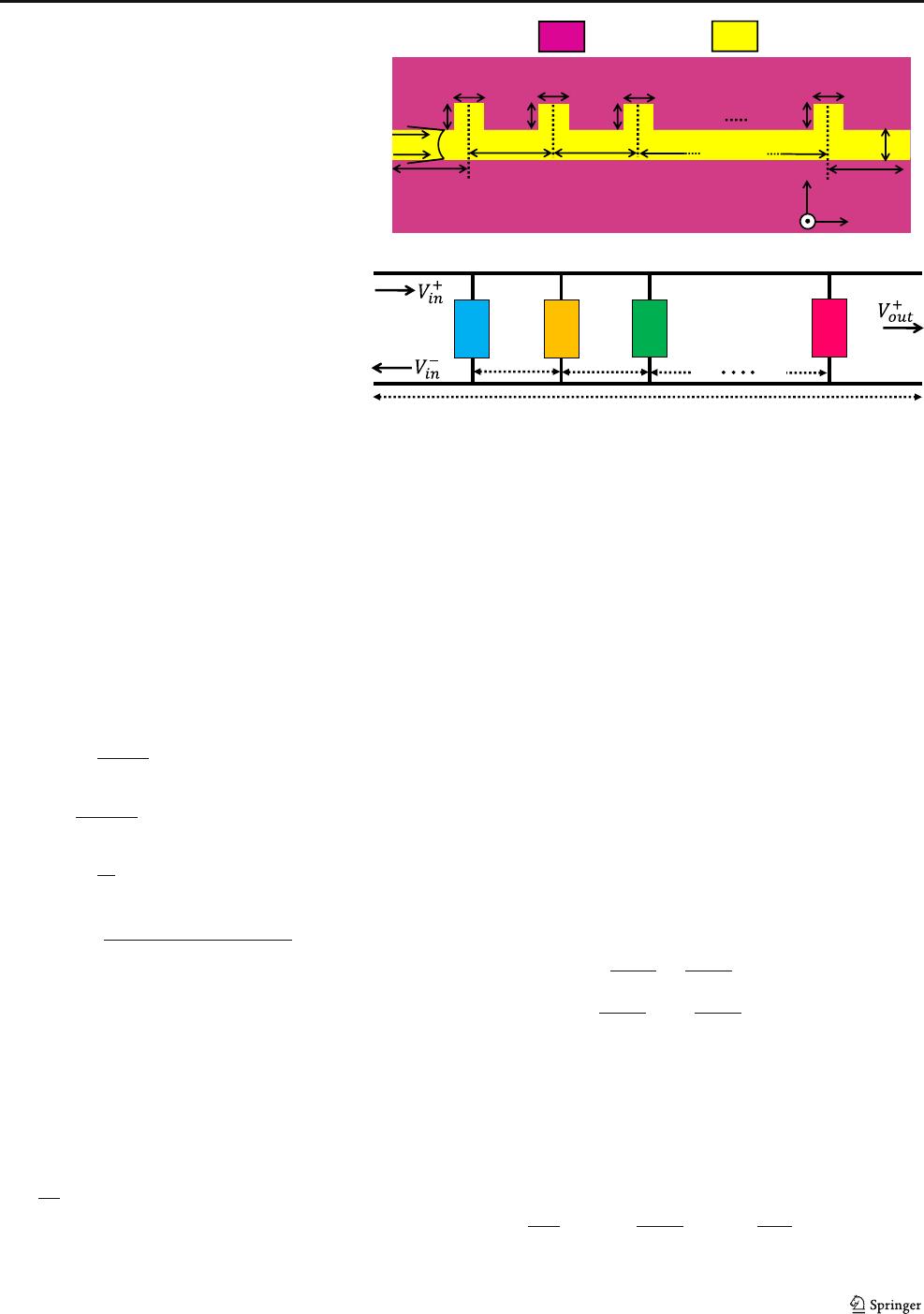
and switches [24]. The equivalent transmission line model
for Fig. 2a is presented in Fig. 2b [54– 56]. It can be seen
that the MDM waveguide is modeled by an infinite trans-
mission line with the characteristic impedance of Z
MDM
.
Also, each of stubs (stub
1
to stub
N
) is modeled by finite
transmission line with the characteristic impedance of Z
S
terminated by a load Z
L
. The total characteristic impedance
of each stub is shown by an effective impedance dubbed as
Z
stub
. The values of the characteristic impedances can be
calculated using Eqs. (5)–(8).
Z
MDM
wðÞ¼
β wðÞw
ωɛ
0
ɛ
1
ð5Þ
Z
s
d
j
¼
β d
j
d
j
ωɛ
0
ɛ
1
: j ¼ 1:2:…:N ð6Þ
Z
L
d
j
¼
ffiffiffiffiffi
ɛ
2
ɛ
1
r
Z
s
d
j
: j ¼ 1:2:…:N ð7Þ
Z
stub j
¼ Z
s
d
j
Z
L
d
j
−iZ
s
d
j
tan β d
j
d
j
Z
s
d
j
−iZ
L
d
j
tan β d
j
d
j
: j ¼ 1:2:…:N
ð8Þ
The propagation constant β can be defined as follows:
β lðÞ¼K n
eff
lðÞ ð9Þ
where l is the width of the waveguide (w for β(w)) or the width
of the stubs (d
j
for β(d
j
)) and K can be derived from Eq. (10):
K ¼
2π
λ
; λ ¼ 2πc=ω ð10Þ
The c parameter is the light speed in vacuum.
Now, there are all the factors to calculate the transfer func-
tion of an MDM waveguide with stub structures. Such a trans-
fer function can be obtained using the transfer matrix method
(Eqs. (11)and(12)) [57, 58]:
V
þ
in
V
−
in
¼ T
V
þ
out
0
ð11Þ
T ¼ A s
1
ðÞB Z
stub1
ðÞA s
2
ðÞB Z
stub2
ðÞ…B Z
stubN
ðÞA s
Nþ1
ðÞ
¼ ∏
N
i¼1
A s
j
B Z
stubj
A s
Nþ1
ðÞ ð12Þ
where the transfer matrix of a straight MDM waveguide with
the length of s
j
(A(s)) and the transfer matrix of a stub with the
length of h
j
(B(Z
stub
)) are defined as follows:
A sðÞ¼
exp −iβsðÞ 0
0expiβsðÞ
ð13Þ
B Z
stub
ðÞ¼
1 þ
Z
MDM
2Z
stub
Z
MDM
2Z
stub
−
Z
MDM
2Z
stub
1−
Z
MDM
2Z
stub
2
6
4
3
7
5
ð14Þ
To verify the aforementioned equations, a simple case is
investigated. The transmitta nce of an MDM waveguide
coupled to a single stub has been calculated (Eq. (15)). Here,
the stub width is considered equal to the width of the MDM
waveguide.
T
1
¼
V
þ
out
V
þ
in
2
¼ 1 þ
Z
MDM
2Z
stub
−2
exp −
L
L
SPP
ð15Þ
Silver
Air
SPPs
x
y
z
w
s
2
s
3
d
1
h
1
d
2
h
2
d
3
h
3
d
N
h
N
s
1
s
N+1
Z
stub1
Z
stub2
Z
stub3
Z
stubN
L
s
1
s
2
(a)
(b)
Fig. 2 a Layout of an MDM
waveguide with N stubs. b
Equivalent transmission line
model
Plasmonics
where L
SPP
is the characteristic propagation length of the SPP
mode and given by Eq. (16).
L
SPP
¼
1
2Im βðÞ
ð16Þ
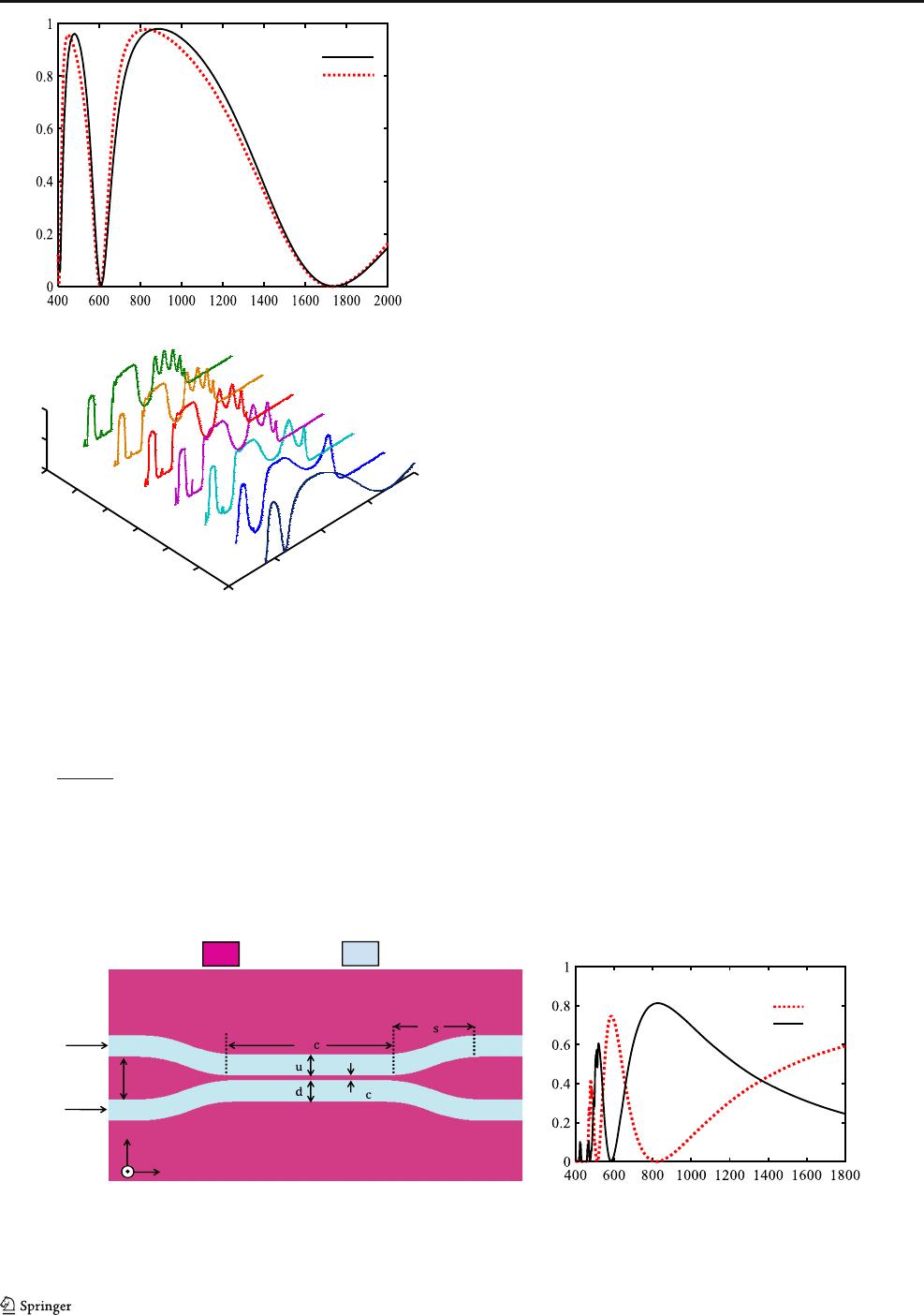
Figure 3a shows the transmittance spectrum of a single stub
structure using TLM and FDTD methods. The dimensions of
the structure are as follows: h
1
= 300 nm, d
1
= 50 nm, w =
50 nm, and L = 400 nm. It can be seen that the transfer func-
tion formula (Eq. (15)) obtained from TLM method confirms
the FDTD results. Figure 2b depicts the transmission spectrum
for when several stubs are connected to the main waveguide
(see Fig. 2a). Here, a distance of 400 nm has been assumed
between the waveguides. As seen, when the number of stubs
is increased, bandgaps are formed in the transmission spec-
trum. Increasing the number of stubs in such a Bragg grating
results in sharper transition region between the permissible
bands and the stop bands. Due to the inherent loss of silver,
using a large number of stubs results in obtaining lower trans-
mittance values.
Design of an AOS Using an Asymmetric DC
First, the transmission spectrum of a conventional plasmonic
DC (Fig. 4) has been investigated. The DC is filled with a
Kerr-type nonlinear material (Ag/BaO). The refractive index
of the Kerr material can be expressed as follows:
n ¼ n
0
þ n
2
I ð17Þ
where n = 1.41 denotes the linear refractive index, n
2
=1.26×
10
−11
cm
2
/W represents the nonlinear refractive index coeffi-
cient, and I is the pumping beam intensity. The substrate metal
is, as mentioned, silver, and the Drude model (Eq. (1)) has
been used for its numerical characterization. The parameter
values of the DC are as follows: L
c
=1080nm,L
s
= 600 nm,
W
u
=W
d
=100nm,g
c
= 20 nm, and g = 300 nm.
As seen in Fig. 4a, the central region of the DC is composed
of two coupled straight MDM waveguides. When two wave-
guides are coupled, light propagating in one of the waveguides
can be coupled to another after passing the coupling length.
Consequently, if a light source is placed on input
1
port, the
transmittance spectra of output
1
(T
11
) and output
2
(T
12
)ports
can be calculated using FDTD method as seen in Fig. 4b.
0
500
1000
1500
2000
1
2
3
4
5
6
7
0
0.5
1
Wavelength (nm)
Number of stubs
ecnattimsnarT
TLM method
FDTD method
Wavelength (nm)
ecnattims
n
a
r
T
(a)
(b)
Fig. 3 Transmittance s pectra of an MDM waveguide wit h (a) a single
stub using TLM an d FDT D met hods . b Differentnumberofstubs
using TLM
Silver
Kerr material
Input
1
L
Output
1
Output
2
w
w
g
L
g
x
y
z
Input
2
T
11
T
12
Wavelength (nm)
ecnat
t
imsnarT
(a) (b)
Fig. 4 a Layout of a typical DC with Lc = 1080 nm, Ls = 600 nm, Wu = Wd = 100 nm, gc = 20 nm, and g = 300 nm. b Its transmission spectra
Plasmonics
Where T
ij
represents the transmittance curves from input
i
to
output
j
. As seen, the incident light for some of the
wavelengths only can pass through one of the output ports.
To clarify the operation mechanism of the DC at different
wavelengths, the field profiles of Re(H
z
) for wavelengths of
585 nm, 658 nm, and 820 nm are shown in Fig. 5 a, b, and c,
respectively. It should be noted that in Fig. 5, based on various
coupling lengths for each wavelength, the wavelengths of
585 nm and 820 nm (Fig. 5 a and c) can pass through the
output
1
and output
2
ports, respectively. Also, the wavelength
of 658 nm (Fig. 5b) can pass through both outputs equally. It is
worth mentioning that if the light source is placed on the
second port, the transmittance spectra of the output ports are
reversed. In other words, T
11
and T
22
and also T
12
and T
21
are
the same.
After the investigation of a conventional DC operation, an
AOS base on asymmetric structure will be d esigned. In
Fig. 6a, the overall structure of the designed AOS is intro-
duced. As seen, the proposed structure consists of a DC loaded
by three stubs, filled with a Kerr nonlinear material (Ag/BaO).
The values of the AOS parameters will be later summarized in
a table in the “Increasing the Number of Stubs” section.
The normalized transmission spectra for T
11
,T
22
,T
12
,
and T
21
are shown and comp ared with each other in
Figs. 6b–c.AsseenfromtheT
11
spectrum, a bandgap with
sharp edges is created in the wavelength range of 710–
957 nm. The wavelength of 740 nm (edge of the bandgap)
can be selected as the data signal wavelength. Since T
11
and T
12
are close to zero at this wavelength, the signal light
cannot pass through the structure, and the AOS is at “off”
-1.3 -1.1 -0.9 -0.7 -0.5 -0.3 -0.1 0.1 0.3 0.5 0.7 0.9 1.1 1.3
X(nm)
× 10
-3
300
100
-100
-300
)mn(y
-3
-2
-1
0
1
2
3
× 10
3
-1.3 -1 -0.7 -0.4 -0.1 0.2 0.5 0.8 1.1 1.3
X(nm)
× 10
3
× 10
-3
-3
-2
-1
1
2
3
0
300
100
-100
-300
)mn(y
-1.3 -1.1 -0.9 -0.7 -0.5 -0.3 -0.1 0.1 0.3 0.5 0.7 0.9 1.1 1.3
X(nm)
× 10
-3
300
100
-100
-300
)mn(y
-3
-2
-1
0
1
2
3
× 10
3
(a)
(b)
(c)
Fig. 5 The field profiles of Re(Hz) for the DC at wavelengths of (a)
585 nm, (b) 658 nm, and (c)820nm
Silver
Kerr material
Signal
light
Pump
light
Output
1
Output
2
L
L
w
w
g
g
d
h
s
x
y
z
T
11
T
12
T
21
T
22
Wavelength (nm)
Transmittance
Wavelength (nm)
e
cn
att
imsn
a
rT
(a)
(b) (c)
Fig. 6 a Layout of the switch 1, b
T11, T12, and c T21, T22
Plasmonics
state in this case (without applying the pump). By applying
the pump light source alone to input
2
, it is observed that the
wavelength of 945 nm almost completely passes through
output
2
and cannot penetrate to output
1
. Examining T
22
and T
21
confirms this fact. Therefore, the wavelength of
945 nm can be used as a pump wavelength.
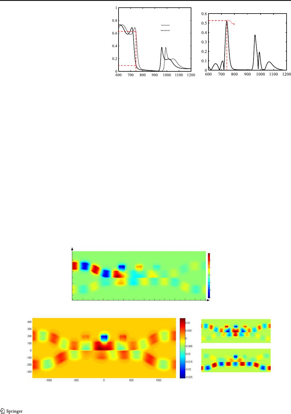
As reviewed, if the data signal source is applied alone, the
switch is at “off” state. However, if in addition to the signal
source, the pump source is also applied (with the pump inten-
sity of I = 3968 MW/cm
2
); the refractive index of the Kerr
region can increase from 1.41 to 1.46. Consequently, the trans-
mittance spectrum of T
11
is shifted to the higher wavelengths
(Fig. 7a). In such a case, the data signal will be able to prop-
agate to the output port. By subtracting the curves in Fig. 7a,
the curve of Fig. 7b is obtained. It should be noted that the
maximum difference is equal to 0.53 which occurs at the
wavelength of 740 nm (the switching wavelength).
The operation of the designed AOS can be also explained by
the magnetic field profile. Figure 8a shows the field profile of
Re(H
z
) at the wavelength of 740 nm in the absence of the pump
light source. As seen, the SPP wave is completely blocked to
the output ports, and the AOS is at the “of f” state. The trans-
mittance of the output
1
port is 0.14 in this state. Figure 8b shows
the field profile of Re(H
z
) when both data and pump signals are
present. The profile of Re(H
z
)inthiscaseisthesummationof
pump signal at the wavelength of 945 nm and the data signal at
the wavelength of 740 nm. As seen in this figure, the incident
light can pass through the structure. The transmittance of the
output
1
port is 0.67 in this case.
After the design of the AOS, some parameter values in-
cluding h
3
and g
c3
have been swept to investigate the effect
of such parameters on the transmittance spectrum of output
1
port. Figure 9a shows the transmittance spectra of output
1
port
for different lengths of the stubs (h
3
). According to this figure,
Pump off
Pump on
Wavelength (nm)
ecna
ttimsna
rT
λ=740 nm
(T
2
-T
1
)
Out1
=0.53
Wavelength (nm)
Transmittance
(a) (b)
Fig. 7 a Transmittance spectra of
output1 without (solid line) and
with (dash line) the pump light. b
The subtraction result of two
transmittance spectra in (a)
X(nm)
mn(y )
Switch on
4
2
0
-2
-4
-6
Switch off
-1.3 -1.1 -0.9 -0.7 -0.5 -0.3 -0.1 0.1 0.3 0.5 0.7 0.9 1.1 1.3
X(nm)
300
100
-100
-300
)
mn(y
× 10
3
× 10
-3
(a)
(b)
=
+
Fig. 8 Field profile of Re(Hz) for switch 1. a With only data source at the wavelength of 740 nm (“off” state). b With pump and data signals both present
Plasmonics
the maximum and minimum transmittances at the wave-
lengths of 710 nm (point A) and 740 nm (point B) correspond
to the h
3
length of 90 nm. In other words, the stub lengths of
90 nm provide the fastest transition from the maximum trans-
mittance to the minimum transmittance. Therefore, it can be
said that h
3
= 90 nm generates the sharpest response.
Another parameter whose variation has been investigated is
the coupling space between the two straight waveguides (g
c3
).
As seen in Fig. 9b, based on the distance between two points
of A and B at wavelengths of 710 nm and 740 nm, g
c3
=20nm
creates the best response to the design of AOS. Other param-
eters are also optimized in a similar way.
Increasing the Number of Stubs
The purpose of this section is that the effe ct of the number of
stubs on AOS operation be investigated. Accordingly , AOSs
named as switch 2 to switch 5 which are composed of four to
seven stubs have been designed as seen in Fig. 10a–d.Theop-
timized structural parameters of the AOSs are given in T able 1.
The operation mechanisms of switch 2 to switch 5 are
similar to switch 1 which is explained in the previous section.
The transmittance spectra of T
11
(the transmittance spectrum
with only signal light source) and T
22
(the transmittance spec-
trum with only pump light source) are shown in Fig. 11a–d.
As seen, if the number of stubs is increased, the edges of the
bandgaps of T
11
curves will be sharper. Consequently, less
pump beam intensity is required to change the refractive index
of the Kerr medium for AOSs with more number of stubs. The
peaks at the wavelengths of 896 nm, 1060 nm, 963 nm, and
1031 nm have been considered as the pump wavelengths for
switch 2 to switch 5, respectively (red dash curves in Fig. 11).
Figure 12 shows the transmittance spectra of output
1
ports
of switch 2 to switch 5 at different pump beam intensities
(pump off and pump on). The pump beam intensities are
3968 MW/cm
2
for switch 2 and 2380 MW/cm
2
for switch 3,
switch 4, and switch 5. The switching wavelengths of switch 2
to switch 5 are shown in Fig. 12 which are equal to 708 nm,
1025 nm, 697 nm, and 736 nm, respectively. Also, the amount
of the transmittances of output
1
ports for switch 2 to switch 5
in “on” and “off” states is given in Table 2.
Wavelength (nm)
Transmission
h
3
(nm)
A
B
710 nm
740 nm
Wavelength (nm)
Transmission
g
c3
(nm)
A
B
710 nm
740 nm
(a)
(b)
Fig. 9 Transmittance spectra of
the switch 1 for different values of
(a)h3and(b)gc3
Silver
Kerr material
Signal light
Pump light
Output
1
Output
2
g
L
L
w
w
g
d
h
s
x
y
z
Silver
Kerr material
Signal light
Pump light
Output
1
Output
2
g
L
L
w
w
d
h
g
s
x
y
z
Silver
Kerr material
Signal light
Pump light
Output
1
Output
2
L
L
w
w
h
d
s
g
g
x
y
z
Silver
Kerr material
Signal light
Pump light
Output
1
Output
2
L
L
s
g
w
w
h
d
g
x
y
z
(a)
(b)
(c)
(d)
Fig. 10 Layout of the (a)switch2,(b)switch3,(c) switch 4, and (d)
switch 5
Plasmonics
Comparisons and Discussions
To have a better view of the obtained results, the perfor-
mance of the proposed AOSs is compared w ith other works
in this section. In Table 2, the investigated characteristics,
including the topology of the AOSs, the Kerr material
along with its nonlinear refractive index coefficient (n
2
),
variations of the linear refract ive index (Δn), the pumping
beam intensity (I), switching wavelengths (λ) wit h their
transmittances for “on” and “off” states (T (On/off)), and
the switch sizes, are provided.
The proposed AOSs provides two isolated input ports for
the signal and pump light sources, while other structures have
a common input port for two sources. The pumping beam
intensity is determined based on two factors including the
Table 1 Dimensions of the designed AOSs (all in nm)
Switch 1
parameters
(three stubs)
Switch 2
parameters
(four stubs)
Switch 3
parameters
(five stubs)
Switch 4
parameter
(six stubs)
Switch 5
parameters
(seven stubs)
L
c3
1080 L
c4
1100 L
c5
2200 L
c6
2100 L
c7
2550
L
s3
600 L
s4
600 L
s5
650 L
s6
600 L
s7
600
g
c3
20 g
c4
20 g
c5
20 g
c6
20 g
c7
20
g
3
300 g
4
300 g
5
150 g
6
110 g
7
200
W
u3
100 W
u4
100 W
u5
100 W
u6
100 W
u7
100
W
d3
100 W
d4
100 W
d5
100 W
d6
100 W
d7
100
S
3
340 S
4
300 S
5
370 S
6
330 S
7
340
d
3
100 d
4
100 d
5
100 d
6
100 d
7
100
h
3
90 h
4
90 h
5
90 h
6
70 h
7
90
Wavelength (nm)
cnattimsnarT
e
T
11
T
22
Wavelength (nm)
Transmittance
T
11
T
22
Wavelength (nm)
cnattimsnarT
e
Wavelength (nm)
Transmittance
T
11
T
22
T
11
T
22
(a)
(b)
(c)
(d)
Fig. 11 Transmittance spectra of output ports for (a)switch2,(b)switch3,(c) switch 4, and (d)switch5
Plasmonics
transmittance spectrum of AOS and the Kerr material used. If
a high quality factor (Q-factor) filter or a structure with to
sharp edges is used, a low pumping light intensity is needed
to change the refractive index of Kerr material. Also, based on
Eq. (17), Kerr materials with higher nonlinear refractive index
coefficient need lower pumping light intensities. Therefore, it
is reasonable that in addition to the pumping light intensity,
the n
2
and Δn of the Kerr materials are compared too. As seen
in Table 2, Δn and I of the designed switches are suitable
compared with the other works.
Other parameters are the switching wavelengths with their
transmittances for “on” and “off” states. It should be noted that
except for [31, 34], switch 2 has the most contrast ratio be-
tween the transmittances of the “on” and “off” states. The
sizes of the switch 1 and 2 are smaller than some structures
such as [59 ]. It should be noted that there is a trade-off
Wavelength (nm)
ecnattimsnarT
Pump off
Pump on
Wavelength (nm)
Transmittance
Pump off
Pump on
Wavelength (nm)
ecnattimsnarT
Pump off
Pump on
Wavelength (nm)
Transmittance
(a)
(b)
(c)
(d)
Fig. 12 Transmittance spectra of
output1 without (solid line) and
with (dash line) pump light for (a)
switch 2, (b)switch3,(c) switch
4, and (d)switch5
Table 2 Performance comparison between the designed AOSs and other works
Ref. Topology Kerr
material
n
2
(cm
2
/W) ΔnI(MW/cm
2
) λ (nm) T (on/off) Size
(nm
2
)
[31] Filter based on disk resonator Au/SiO
2
2.7×10
−9
0.13 48.31 980 0.73/0.02 908×368
[32] Filter based on disk
and stub resonators
Ag/BaO 1.26×10
−11
0.022 1746 563 0.5/0.03 795×505
[34] Filter based on ring resonator InGaAsP 1×10
−12
0.016 1668 872 0.82/0.12 690×320
[59] Filter based on ring resonator Ag/BaO 1.26×10
−11
0.22 17,140 850 0.53/0.012 975×610
[59] Filter based
on double ring resonators
Ag/BaO 1.26×10
−11
0.058 4600 1490&1550&1590 0.46/0.002 & 0.3/0.04 &
0.54/0.05
975×1000
[60] Filter based on ring resonator Ag/BaO 1.26×10
−11
0.016 127 1545 0.58/0.023 1136×537
Switch 1 Asymmetric DC Ag/BaO 1.26×10
−11
0.05 3968 740 0.67/0.14 2680×310
Switch 2 Asymmetric DC Ag/BaO 1.26×10
−11
0.05 3968 708 0.715/0.07 2700×310
Switch 3 Asymmetric DC Ag/BaO 1.26×10
−11
0.03 2380 1025 0 .482/0.05 3900×310
Switch 4 Asymmetric DC Ag/BaO 1.26×10
−11
0.03 2380 697 0.442/0.045 3800×290
Switch 5 Asymmetric DC Ag/BaO 1.26×10
−11
0.03 2380 736 0.53/0.08 4150×310
Plasmonics

between designing parameters of AOSs. Increasing the num-
ber of stubs in our deign leads to less required pumping power.
Conclusion
In summary, a novel topology for all optical plasmonic
switches was proposed. It is based on an asymmetric di-
rection coupler on which Bragg grating is applied. Ag/BaO
composite and silver are the composing materials of this
switch. The proposed structures were numerically simulat-
ed using FDTD method. The proposed structures provide
different input and output ports for the data and pump
signals, and hence, they have the potential to be used in
highly integrated optical circuits.
References
1. Liu L, Han Z, He S (2005) Novel surface plasmon waveguide for
high integration. Opt Express 13(17):6645–6650
2. Geravand A, Danaie M, Mohammadi S (2019) All-optical photonic
crystal memory cells based on cavities with a dual-argument hys-
teresis feature. Opt Commun 430:323–335
3. Danaie M, Kiani B (2018) Design of a label-free photonic crystal
refractive index sensor for biomedical applications. Photonics and
Nanostructures-Fundamentals and Applications 31:89–98
4. Danaie M, Nasiri Far R, Dideban A (2018) Design of a high-
bandwidth Y-shaped photonic crystal power splitter for TE modes.
International Journal of Optics and Photonics 12(1):33–42
5. Nasirifar R, Danaie M, Dideban A (2019) Dual channel optical
fiber refractive index sensor based on surface plasmon resonance.
Optik 186:194–204
6. Moradi M, Danaie M, Orouji AA (2018) Design and analysis of an
optical full-adder based on nonlinear photonic crystal ring resona-
tors. Optik 172:127–136
7. Janković N, Cselyuszka N (2019) High-resolution plasmonic filter
and refractive index sensor based on perturbed square cavity with
slits and orthogonal feeding scheme. Plasmonics 14(3):555–560
8. Khani S, Danaie M, Rezaei P (2019) Design of a single-mode
plasmonic bandpass filter using a hexagonal resonator coupled to
graded-stub waveguides. Plasmonics 14(1):53–62
9. Khani S, Danaie M, Rezaei P (2018) Realization of single-mode
plasmonic bandpass filters using improved nanodisk resonators.
Opt Commun 420:147–156
10. Chang Y, Jiang Y (2014) Highly sensitive plasmonic sensor based
on Fano resonance from silver nanoparticle heterodimer array on a
thin silver film. Plasmonics 9(3):499–505
11. Danaie, M., & Shahzadi, A. (2019). Design of a high-resolution
metal–insulator–metal plasmonic refractive index sensor based on
a ring-shaped Si resonator. Plasmonics, 1-13
12. Geng XM, Wang TJ, Yang DQ, He LY, Wang C (2016) Tunable
plasmonic wavelength demultiplexing device using coupled reso-
nator system. IEEE Photonics Journal 8(3):1–8
13. Khani S, Danaie M, Rezaei P (2018) Double and triple-wavelength
plasmonic demultiplexers based on improved circular nanodisk res-
onators. Opt Eng 57(10):107102
14. Chen Z, Chen M, Li J, Wang L, Jiao R, Duan G, Xiao J (2016)
Symmetry breaking induced mode splitting based on a plasmonic
waveguide system. J Phys D Appl Phys 49(14):145109
15. Dolatabady A, Granpayeh N (2017) Plasmonic directional couplers
based on multi-slit waveguides. Plasmonics 12(3):597–604
16. Liang S, Jiang C, Yang Z, Li D, Zhang W, Mei T, Zhang D (2018)
Plasmonic slow light waveguide with hyperbolic metamaterials
claddings. J Opt 20(6):065001
17. Khani S, Danaie M, Rezaei P (2019) Tunable single-mode
bandpass filter based on metal–insulator–metal plasmonic coupled
U-shaped cavities. IET Optoelectron
18. Khani S, Danaie M, Rezaei P (2019) Size reduction of MIM surface
plasmon based optical bandpass filters by the introduction of arrays
of silver nano-rods. Physica E: Lo w-dimensional Systems and
Nanostructures 113:25–34
19. Khani, S., Danaie, M., Rezaei, P., & Shahzadi, A. (2019). Compact
ultra-wide upper stopband microstrip dual-band BPF using tapered
and octagonal loop resonators. Frequenz, accepted
20. Khani S, Hayati M (2017) Compact microstrip lowpass filter with
wide stopband and sharp roll-off. Microw J 60(11)
21. Khani S, Mousavi SMH, Danaie M, Rezaei P (2018) Tunable com-
pact microstrip dual-band bandpass filter with tapered resonators.
Microw Opt Technol Lett 60(5):1256–1261
22. Khani S, Danaie M, Rezaei P (2019) Miniaturized microstrip dual-
band bandpass filter with wide upper stop-band bandwidth. Analog
Integr Circ Sig Process 98(2):367–376
23. Khani S, Makki SVAD, Mousavi SMH, Danaie M, Rezaei P (2017)
Adjustable compact dual-band microstrip bandpass filter using T-
shaped resonators. Microw Opt Technol Lett 59(12):2970–2975
24. Taheri AN, Kaatuzian H (2014) Design and simulation of a nano-
scale electro-plasmonic 1× 2 switch based on asymmetric metal
–
insulator–metal stub filters. Appl Opt 53(28):6546–6553
25. Krasavin AV, Zayats AV (2010) Electro-optic switching element for
dielectric-loaded surface plasmon polariton waveguides. Appl Phys
Lett 97(4):041107
26. Zhu JH, Huang XG, Mei X (2011) Plasmonic electro-optical
switches operating at telecom wavelengths. Plasmonics 6(3):605
27. Tsilipakos O, Kriezis EE, Bozhevolnyi SI (2011) Thermo-optic
microring resonator switching elements made of dielectric-loaded
plasmonic waveguides. J Appl Phys 109(7):073111
28. Qi Z, Hu G, Yun B, Zhang X, Cui Y (2016) Fast response and low
power consumption 1× 2 thermo-optic switch based on dielectric-
loaded surface plasmon polariton waveguides. J Mod Opt 63(14):
1354–1363
29. Liu Y, Bartal G, Genov DA, Zhang X (2007) Subwavelength dis-
crete solitons in nonlinear metamaterials. Phys Rev Lett 99(15):
153901
30. Wurtz GA, Zayats AV (2008) Nonlinear surface plasmon
polaritonic crystals. Laser Photonics Rev 2(3):125–135
31. Tao J, Wang QJ, Huang XG (2011) All-optical plasmonic switches
based on coupled nano-disk cavity structures containing nonlinear
material. Plasmonics 6(4):753
32. Lu H, Liu X, Wang L, Gong Y, Mao D (2011) Ultrafast all-optical
switching in nanoplasmonic waveguide with Kerr nonlinear reso-
nator. Opt Express 19(4):2910–2915
33. Wang G, Lu H, Liu X, Gong Y (2012) Numerical investigation of
an all-optical switch in a graded nonlinear plasmonic grating.
Nanotechnology 23(44):444009
34. Tian M, Lu P, Chen L, Liu D, Lv C (2012) All-optical switching in
MIM waveguide resonator with an outer portion smooth bend struc-
ture containing nonlinear optical materials. Opt Commun 285(21–
22):4562–4566
35. Chen F, Yao D (2014) Tunable multiple all-optical switch based on
multi-nanoresonator-coupled waveguide systems containing Kerr
material. Opt Commun 312:143–147
36. Ghadrdan M, Mansouri-Birjandi MA (2018) Design and imple-
mentation of optical switches based on nonlinear plasmonic ring
resonators: circular, square and octagon. Photonics and
Nanostructures-Fundamentals and Applications 29:15–21
Plasmonics
