15
Mater. Res. Soc. Symp. Proc. Vol. 1292 © 2011 Materials Research Society
DOI: 10.1557/opl.2011.18
Coupling of Defect Fields to Domains and Phase Transition Characteristics of Ferroelectric
Thin Films with Charged Defects
Ibrahim B. Misirlioglu
1
, Hale N. Cologlu
1
and Mehmet Yildiz
1
1
Faculty of Engineering and Natural Sciences, Sabanci University, Tuzla/Orhanli, 34956
Istanbul, Turkey
ABSTRACT
We analyze the effect of charged defects on the electrical domains, phase transition
characteristics and electrical properties of ferroelectric thin films with thin dead layers using a
non-linear thermodynamic model. Depending on their density and field strength, defects can pin
and couple to electrical domains in the film. For ultrathin films, depolarizing effects dominate
and the transition from the paraelectric state is into the multidomain ferroelectric state during
cooling and is strongly smeared. The competition between defect induced extrinsic effects and
the dead layer related limit is demonstrated.
INTRODUCTION
Phenomena related to inhomogeneities and defects in ferroelectric thin films have been an
interest for the scientific community since more than the last two decades. The impact of defect
fields on the physical properties of ferroelectric films have been the focus of numerous studies
including dedicated book chapters [1-10]. The motivation is to understand the structure-electrical
property relation in these materials that are strong candidates for several electronic applications.
Recently, with the emergence of techniques capable of fabricating very thin films, wherein
the distances through which defect fields permeate become comparable to film thickness, related
effects have gained a special importance. Defects with charges near the surfaces have also been
treated as centers strongly influencing switching characteristics or hinder domain wall motion [9,
18, 19].
An example to the macroscopic effect of a network of defects is the discussions on whether
the disappearance of ferroelectricity in ultrathin films is an intrinsic behavior set by atomistic
mechanisms or caused by interfacial inhomogeneities that put an extrinsic limit on the film
thickness. However, how such an intrinsic limit trend would be modified in the presence of even
a low density of charged defects remains a very interesting question.
In this article, we study the behavior of ferroelectric thin films with charged defects that are
introduced into the system as point potentials, sandwiched between metallic electrodes with dead
layers. To probe the strength of the defect effects we use the Landau-Ginzburg-Devonshire
(LGD) formalism for ferroelectric materials coupled with the interface conditions and defect
fields. Following the simulation of P at 25϶C, we study the phase transition characteristics of the
films both for the chosen thicknesses.

16
THEORY
As the first step, we first construct a two dimensional grid with a sandwich type capacitor
geometry that is 200n x kn cells where k (200) is the number of cells along the film thickness
(width) and each cell, n, has a dimension of 0.4 nm, imitating the unit cell dimensions of PZT.
The LGD volumetric free energy for an epitaxial single domain (001) ferroelectric film on a
(001) cubic substrate can be written as:
[]
dVFwFFFFFwF
V
DLESGEPT
³
−+−+++= )1()(
0
(1)
where w becomes zero in the dead layer and is one in the ferroelectric film. F
0
is the energy of
the paraelectric state and
2
3
2
2
2
1123
2
2
2
1
42
3
2
1
4
2
2
3
2
2
4
1112
6
3
6
2
6
1111
2
3
2
2
2
3
2
1
2
2
2
112
4
3
4
2
4
111
2
3
2
2
2
11
)]()()([)(
)()()(
PPP
PPPPPPPPPPPP
PPPPPPPPPPPPF
z
P
α
αα
ααα
+
+++++++++
++++++++=
(2)
is the energy due to the polarization P
i
(i=1,2,3) in the ferroelectric state.
α
i
,
α
ij
, and
α
ijk
are the
dielectric stiffness coefficients [20]. F
E
is the internal elastic energy both due to the misfit
between the film and the substrate as well as the self-strain given by:
()( )
00
2
1
klklijijijklE
CF
εεεε
−−=
(3)
where C
ijkl
is the elastic stiffness for a cubic crystal, İ
11
=İ
22
is the film-substrate misfit strain in
the pseudocubic limit, İ϶
ij
is the self-strain energy due to the paraelectric-ferroelectric phase
transition in the pseudocubic film. The gradient energy due to variations in P
i
is given by:
2
2
21
2
2
23
2
1
11
2
1
13
2
3
31
2
3
33
¸
¹
·
¨
©
§
+
¸
¹
·
¨
©
§
+
¸
¹
·
¨
©
§
+
¸
¹
·
¨
©
§
+
¸
¹
·
¨
©
§
+
¸
¹
·
¨
©
§
=
dx
dP
G
dz
dP
G
dx
dP
G
dz
dP
G
dx
dP
G
dz
dP
GF
G
(4)
where G
ij
are the gradient energy coefficients and we shall assume that it is isotropic for
convenience, namely G. We also neglect the variations along P
2
along y in the 2D limit. F
ES
is
the electrostatic energy of the system,
iiES
PEF −= where
i
E is found from the Maxwell
equation 0=
i
divD and
i
D are the dielectric displacement components. F
DL
is the energy of the
dead layer that is assumed to be a linear dielectric. Equation (1) is minimized and the
corresponding Euler-Lagrange equations are obtained from where we find the P components in
the system. The dead layer, when present, is assumed to be a high-k dielectric whose dielectric
constant is chosen as 20 with thicknesses as either one or two unit cells when specified.
The boundary conditions we employed for P
3,1
are dP
3
/dz=0 and dP
1
/dx=0 at the top and
bottom electrode-film interface of the ferroelectric layer. The periodic boundary conditions used
along the sides (x-axis) are;
),()0,(
33
LxzPxzP ===
,
),()0,(
11
LxzPxzP ===
(5)
Dirichlet boundary conditions are applied at the dead layer-electrode interface to solve the
fields coupled with P
1,3
. The equations of state are solved simultaneously employing a Gauss-
Seidel iterative scheme subject to boundary conditions mentioned above. We limit ourselves to
5000 iterations converging to a difference of 10
-8
between consecutive iterative P solution steps
when ferroelectricity exists.

17
The paraelectric-ferroelectric phase transition (PT) characteristics are studied through
finding P
3
by varying temperature between RT and 900ºC. These simulations are run for films
that are 6.4 and 14.4 nm thick in the presence and absence of charged defects. At each
temperature, the equations given above are solved for all P components and the resulting
configuration constitued the initial condition for the next step. The thickness of the dead layers in
these runs are also specified when necessary to demonstrate the competition between defect
effects and the dead layer effects. For convenience, we neglect the thermal expansion differences
and fix the value of the pseudocubic misfit in the entire range to solely reveal the PT
characteristics.
The material system considered in this study is heteroepitaxial (001) PZT 30/70 on a (001)
SrTiO
3
(ST) substrate with pseudomorphic top and bottom metallic electrodes. The values of the
dielectric stiffness coefficients and other thermodynamic parameters entering the calculations are
cited from [21]. Simulation results are presented for PZT 30/70 films of 6.4 nm and 14.4 nm.
DISCUSSION
Room temperature domain structures
We start by discussing the stable domain structures of the films at 25ºC for various film
thicknesses with and without defects in the light of our results. The electrodes lie on the
horizontal x-axis while perpendicular axis is denoted as z-axis.
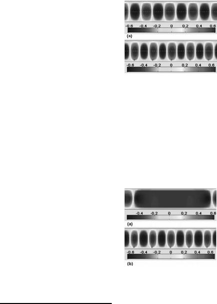
In Figure 1a-b, the color maps of the P
3
at 25ºC for 6.4 nm film are given in the presence
and absence of defects. In the 6.4 nm films, the 180º domains form regardless of the defects. We
obtain the domain period for the defect-free film as 13.33 nm whereas this is 16 nm for the
defected film which is due to the enhancement of P
3
in the vicinity of the defects in which the
order of distances that this enhancement takes place is comparable to the film thickness, favoring
a positive P
3
with the rest of the film coupling to these fields via the electrodes.
The results for the effect of defects on the stability of 180º domains in the 6.4 nm film under
bias are given in Figure 1c-d. A voltage of -0.2 V is applied to the bottom electrode while the
upper electrode is kept at 0 V. In the presence of the bias, there is no change in the defect free
film as it sustains the domain structure with a slightly higher number of switched cells in favor of
the bias field. When defects are present, P
3
in their vicinity is enhanced and this conversely
impacts the number of sites switched. As seen in Figure 1d, there is a significant portion that
have not switched but the behavior is still comparable to that of the defect-free 6.4 nm film. On
the other hand, the domain period, in both films remains nearly constant under -0.2 V bias. An
applied field opposing the sign of the defect induced field has to have values higher than those
for a defect-free film to induce complete switching.
Figure 1. The 25°C domain configurations of the 6.4 nm thick film with dead layers for (a)
defect-free film, (b) the film with charged defects near the bottom electrode, (c) defect-free film
under -0.2V bias (d) film with defects under -0.2V bias. Throughout the figures, scales are given
to display the range of P
3
in C/m
2
.
18
In Figure 2a-b we provide the results for the 14.4 nm films with two unitcell thick dead
layers. The domains are stable in both defected and defect-free cases at zero bias. The domain
period for the defect free film is interestingly larger than that of the defected film, where the
former has 20 nm periods and the latter has 16 nm. This is just the opposite of the 6.4 nm case.
Considering the magnitude of the jump at the ferroelectric-dead layer interface that determines
the amount of partially compensated bound charges, defects lead to an overall enhancement of P
3
in the film accompanied by a growing density of bound charges at the film-dead layer interface,
with a smaller period multidomain sequence to minimize the depolarizing fields. So, the 14.4 nm
film is under the influence of an enhanced depolarizing field due to the bias induced by defects
instead of a strong thickness effect mostly pronounced in ultrathin films.
Figure 2. The 25°C domain configurations of the 14.4 nm thick film with dead layer dielectric
constant İ=20 for (a) defect-free film, (b) the film with charged defects near the bottom
electrode.
In the 14.4 nm thick film, upon applying a -0.2 V bias to the bottom electrode, the defect-
free film has switched (Fig. 3a), while electrical domains persist in the defected one (Fig. 3b).
There is a near-single domain state under -0.2 V bias in the defect-free 14.4 nm film while the
film with defects has strongly pinned domains, both due to defect fields, sustaining the
multidomain configuration owing to the enhancement of P
3
in the domains through the long-
range effects, and the commensurately larger depolarizing field as well. It is critical here to
notice that the local depolarizing field magnitude will change with variations in the P
3
throughout the film while the defect fields are fixed.
Figure 3. The domains in the 14.4 nm film under -0.2V bias for (a) defect-free film and (b) film
with defects.
Phase transition characteristics
Before we go onto discussing the competition between the intrinsic-extrinsic limit effects,
we computed the P-T curve for perfect 6.4 nm and 14.4 nm films with no dead layers as
reference. The P solutions and T
C
of the two cases is the same and is around 880ºC, near twice
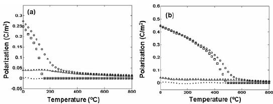
19
the bulk T
C
due to the compressive in-plane misfit and are not shown here for brevity. When
present, dead layers at both electrode-film interfaces are assumed to exist at a thickness of one
unit cell as already mentioned in the 6.4 nm film. We choose so as dead layers that are two unit-
cell thick reduce the T
C
of 6.4 nm film dramatically, to about 80ºC, confining the transition to a
small T region with respect to thicker films. During the simulations, if the transition from the
paraelectric state is into a multidomain ferroelectric state, one can track <|P
3
|> to allow the
detection of the transition point. Figure 4a shows the net P
3
and <|P
3
|> in the 6.4 nm thick film
without and with defects respectively. The transition temperature for the defect free film is
around 150ºC. The film with charged interface defects have a strongly smeared transition in the
150-300ºC range with a non-zero P
3
remaining and gradually leveling off at elevated
temperatures (See |P
3
| and <P
3
> for the defect free film in Figure 4a). The depolarizing field,
when dead layers are present, is quite strong for the 6.4 nm film due to the bound charge induced
potential drop at shorter distances when electrodes are kept at zero potential. Therefore, T
C
is
lowered significantly in the defect-free 6.4 nm film. A multidomain structure with the majority
of the volume having a positive P
3
in favor of the defect fields is stable at low temperatures
(Please see the <P
3
> for the defected films in Figure 4a). One must remember that these films are
also under the influence of a size limit via the depolarizing field taking effect in the presence of
dead layers.
Figure 4. P-T curves for (a) the defect-free and defected 6.4 nm thick film and (b) defect-free
and defected 14.4 nm thick film. Squares: <|P
3
|> for defect-free film, open circles: <|P
3
|> for
defected film, solid small circles: <P
3
> for defect-free film, triangles: <P
3
> for defected film in
both (a) and (b).
From Figure 4b, the paraelectric-ferroelectric transition temperature for the defect-free 14.4
nm film with 2 unit-cell thick dead layers is around 500ºC and into a multidomain state during
cooling. Throughout the whole temperature range, there is a non-zero, positive P
3
when defects
are present that implies the presence of a built-in P
3
. Similar results have been recently obtained
for thick (200 nm) single domain PZT 30/70 that does not have any dead layers but high
densities of continuous space charge distribution near one of the electrodes [21]. A stronger
smearing in the 6.4 nm film is resulting from the fact that the defect fields are much stronger due
to the film thickness, causing steeper potential drops that induce larger electric fields.
CONCLUSIONS
We have demonstrated the competition between the defect induced electrostatic fields with
the depolarizing fields due to dead layers is most prominent in the ultrathin films. Frozen-in
20
defect fields could strongly pin the domains in ultrathin films by electrostatic means, reducing
the switchable P
3
. The 14.4 nm film turns out to have potentially more stable P
3
and it seems that
the thicker films the less likely they will be under the influence of charged defects. During near-
equilibrium cooling, the paraelectric-ferroelectric transition is more prominently smeared in
ultrathin films compared to thicker ones even in the presence of widely seperated charged defect
sites. Still, the depolarizing effects should be expected to compete with defect fields in ultrathin
films in the presence of charged sites as demonstrated. It is obvious that charged defects, when
high in density, can significantly alter the properties but the depolarizing fields also develop
accordingly, dictating the electrical response as well as the domain configuration for films with
dead layers much thicker than a unit cell.
REFERENCES
1. S. Triebwasser, Phys. Rev. 118, 100 (1960).
2. A. P. Levanyuk and A. S. Sigov, “Defects and Structural Phase Transitions”, Volume 6,
in Ferroelectricity and Related Phenomena, edited by W. Taylor, Gordon and Breach
Science Publishers, (1988).
3. W. L. Warren, D. Dimos, G. E. Pike, B. A. Tuttle, M. V. Raymond, R. Ramesh and J. T.
Evans, Appl. Phys. Lett. 67, 866 (1995).
4. T. M. Shaw, S. Troiler-McKinstry, P. C, Mcintyre, Ann. Rev. Mat. Sci. 30, 263 (2000).
5. R. Ramesh, S. Aggarwal and O. Auciello, Mat. Sci. Eng. Rep. 32, 191 (2001).
6. C. S. Ganpule, A. L. Roytburd, V. Nagarajan, B. K. Hill, S. B. Ogale, E. D. Williams, R.
Ramesh and J. F. Scott, Phys. Rev. B 65, 014101 (2002).
7. H. Z. Jin and J. Zhu, J. Appl. Phys. 92, 4594 (2002).
8. M.-W. Chu, I. Szafraniak, R. Scholz, C. Harnagea, D. Hesse, M. Alexe and U. Gösele,
Nat. Mater. 3, 87 (2004).
9. X. Ren, Nat. Mater. 3, 91 (2004).
10. (9.5) E. Cockayne and B. P. Burton, Phys. Rev. B, 69, 144116 (2004).
11. D. Balzar, P. A. Ramakrishnan and A. M. Hermann, Phys. Rev. B 70, 092103 (2004).
12. S. P. Alpay, I. B. Misirlioglu, V. Nagarajan, R. Ramesh, Appl. Phys. Lett. 85, 2044
(2004).
13. Y. Xiao, V. B. Shenoy and K. Bhattacharya, Phys. Rev. Lett. 95, 247603 (2005).
14. W. Laguta , A. M. Slipenyuk, I. P. Bykov, M. D. Glinchuk, M. Maglione, D. Michau, J.
Rosa, and L. Jastrabik, Appl. Phys. Lett. 87, 022903 (2005).
15. Y. Zheng, B. Wang and C. H. Woo, Appl. Phys. Lett. 88, 092903 (2006).
16. I. B. Misirlioglu, Mark Aindow, S. P. Alpay, and V. Nagarajan, Appl. Phys. Lett. 88,
102906 (2006).
17. Y. L. Li, S. Y. Hu, S. Choudhury, M. I. Baskes, A. Saxena, T. Lookman, Q. X. Jia, D. G.
Schlom and L. Q. Chen, J. Appl. Phys. 104, 104110 (2008).
18. S. V. Kalinin, S. Jesse, B. J. Rodriguez, Y. H. Chu, R. Ramesh, E. A. Eliseev and A. N.
Morozovska, Phys. Rev. Lett. 100, 155703 (2008).
19. D. Schrade, B.X. Xu, R.Muller and D. Gross, Proc. Appl. Math. Mech. 7, 4040015
(2007).
20. M. J. Haun, Z. Q. Zhuang, E. Furman, S. J. Jang, L. E. Cross, Ferroelectrics 99, 45
(1989).
21. I. B. Misirlioglu, M. B. Okatan and S. P. Alpay, J. Appl. Phys.108, 034105 (2010).
