Electrical response of polycrystalline silicon thin film transistor on
steel foil under mechanical strain
Po-Chin Kuo, Abbas Jamshidi-Roudbari and Miltiadis K. Hatalis
Electrical and Computer Engineering, Lehigh University, Bethlehem, PA, 18015
ABSTRACT
This work investigates the effects of mechanical strain on electrical characteristics of
polycrystalline thin film transistors (poly-Si TFTs). Poly-Si TFTs were fabricated on steel foil
substrate and characterized under the strain ranging from -1.2% to 1.1% induced by bending.
The electron mobility increased under tensile and decreased under compressive strain while that
of the hole exhibited an opposite trend. For p-channel TFTs the normalized threshold voltage and
subthreshold slope were a function of strain. In both n- and p-channel TFTs the off current
decreased under tensile while it increased under compressive strain. The observed mobility and
off current trends in poly-Si TFTs under strain are similar to those reported in single crystalline
silicon devices.
INTRODUCTION
Mechanically flexible electronic systems have the potential to realize novel applications and
thus have recently attracted a lot of research interest. Most of the reported flexible electronics are
based on amorphous silicon thin film transistor (a-Si:H TFT) technology because this technology
is deemed more readily compatible with flexible polymer substrates. However, the low carrier
mobility in amorphous silicon and the poor reliability of amorphous silicon TFTs may limit the
applications of this technology. Polycrystalline silicon thin-film transistor (poly-Si TFT)
technology on steel foils has been successfully demonstrated as a platform for high performance
flexible electronics [1] because of the high electron and hole mobility that enables CMOS circuit
architectures and the compatibility of this technology with high processing temperatures. High
resolution flexible displays have also been realized by this technology [2].
One of the most important features of any flexible electronic system is its ability to be
deformed. However, any form of deformation induces mechanical strain to the electronic thin
film devices and circuits fabricated on the flexible substrate. Therefore it is necessary to
understand the effects of mechanical strain on the electrical characteristics of thin film devices.
There are extensive studies over a-Si:H TFTs [3, 4] and also organic TFTs [5] on flexible
substrate under mechanical strain. The relevant work on poly-Si TFTs was lacking thus in our
earlier effort we investigated the effect of tensile strain on mobility of poly-Si TFTs [6]. To make
the work more complete in this paper we report the mobilities and characteristics of both n-
channel and p-channel poly-Si TFTs under both uniaxial tensile and compressive strain induced
by bending.
EXPERIMENT
We fabricated arrays of poly-Si TFTs on a 100 µm thick, type 304, 150 mm in diameter
stainless steel substrate. The polished steel wafers had a surface roughness (Ra) of only 10 nm.
The metal foil wafers were coated with a 3 µm thick PECVD SiO
2
passivation layer on both
Mater. Res. Soc. Symp. Proc. Vol. 1116 © 2009 Materials Research Society 1116-I01-05
sides in order to electrically isolate the steel substrate. The active semiconductor layer was 50 nm
of a PECVD deposited amorphous silicon film which was laser crystallized by using the
sequential lateral solidification (SLS) method [7]. After patterning the silicon active layer, a 50
nm thick PECVD SiO
2
layer and a 200 nm thick LPCVD amorphous silicon layer were
deposited as the gate dielectric and the gate electrode layers respectively. The gate electrode
layer was then doped n+ by ion implantation of phosphorus, patterned, and dry etched. The
source and drain regions of n-channel TFTs were then implanted with phosphorous, while those
of p-channel TFTs were implanted with boron. After implantation, an activation anneal at 650 °C
was performed, and then the source, drain and gate regions were silicided using nickel. After
deposition of a PECVD SiO
2
passivation layer, a 300 nm thick aluminum and a 50 nm thick
nickel was deposited and patterned using lift-off. Finally, a post metallization anneal at 350 °C
followed by a plasma hydrogenation anneal at 300 °C were performed. A cross-sectional view of
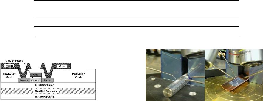
the indented poly-Si TFT structure is shown in figure 1. Initial characteristics of TFTs having a
channel width of 16µm and channel length of 8 µm are shown in Table I. Samples being 20 mm
by 35 mm were then cut from the steel wafers for performing the bending experiments.
We applied tensile as well as compressive strain on poly-Si TFTs by bending the sample
outward and inward to fit the outer and inner surfaces of cylindrical tubes with various radii. To
be accurate for strain calculation, the sample was well constrained to conform to the surface of
the cylinder. The strain ε, was then calculated from the relationship ε = z/R, where R is the
bending radius and z is the distance from the neutral plane to the active layer of the TFT. In our
samples the neutral plane is approximately located in the middle of the stainless steel foil
substrate because the TFT layers are thin (~1µm) compared to the steel foil substrate (~100µm)
and the Young’s modulus of stainless steel is larger than that of the thin film materials.
The equivalent uniaxial strain resulting from the bending was in the range from -1.2% to
1.1% and this strain was parallel to the TFT channel direction in this experiment. Figure 2 shows
the configuration of the experimental setup. Transfer characteristics were measured, at a drain to
source voltage of Vds= 0.1 V for n-channel and Vds= -0.1 V for p-channel TFTs, at each
bending radius from the same TFTs. Field effect mobility, threshold voltage and subthreshold
slope were then extracted from these measurements.
Table I. Poly-Si TFTs characteristics (W/L=16µm/8µm)
Figure 1. Poly-Si TFT structure Figure 2. Characterization of poly-Si TFT under
on stainless steel foil tensile (left) and compressive (right) strain
Type
Mobility
(cm
2
/Vs)
V
th
(V)
Subthreshold slope
(dec/V)
n-channel 310 -0.03 4.9
p-channel 105.8 -2.75 3.8
RESULT AND DISCUSSION
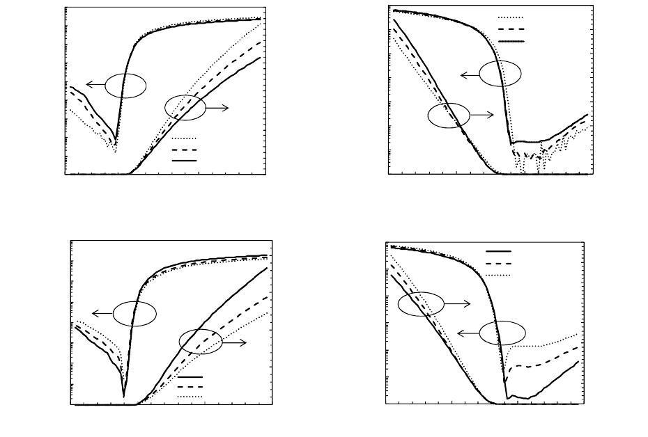
Figure 3 shows the transfer characteristics of n-channel and p-channel poly-Si TFTs for
various tensile and compressive strains. As it can be seen by comparing figure 3(a) and 3(b), the
on current increases while the off current decreases in the n-channel TFTs, whereas both on and
off currents decrease in the p-channel TFTs as the applied tensile strain increases. However, all
these trends are reversed under compressive strain as shown in figure 3(c) and 3(d).
The observed off current trends are similar to those reported for the single crystalline silicon
MOSFET devices and which were attributed to the change of silicon band gap under strain [8, 9]
– the energy bandgap increases under uniaxial tensile and decreases under uniaxial compressive
strain. In poly-Si TFTs the thermionic emission is the dominant mechanism for the off leakage
current [10] at low drain bias. The change of silicon bandgap would affect the barrier height
which carriers in grain boundary traps would have to overcome in order to contribute to TFT off
current. As a result for both n- and p-channel TFTs the off current decreases under tensile and
increases under compressive strain.
0.0E+00
5.0E-06
1.0E-05
1.5E-05
2.0E-05
2.5E-05
3.0E-05
1.0E-13
1.0E-12
1.0E-11
1.0E-10
1.0E-09
1.0E-08
1.0E-07
1.0E-06
1.0E-05
1.0E-04
-5 0 5 10
I
d
(A)
V
G
(V)
Strain= 0.95%
Strain= 0.21%
Strain= 0%
(a)
0.0E+00
1.0E-06
2.0E-06
3.0E-06
4.0E-06
5.0E-06
6.0E-06
7.0E-06
1.0E-12
1.0E-11
1.0E-10
1.0E-09
1.0E-08
1.0E-07
1.0E-06
1.0E-05
-10 -5 0 5
I
d
(A)
V
G
(V)
Strain= 0.95%
Strain= 0.21%
Strain= 0%
(b)
0.0E+00
5.0E-
06
1.0E-
05
1.5E-
05
2.0E-
05
1.0E-12
1.0E-11
1.0E-10
1.0E-09
1.0E-08
1.0E-07
1.0E-06
1.0E-05
1.0E-04
-5 0 5 10
I
d
(A)
V
G
(V)
Strain= 0%
Strain=- 0.56%
Strain=- 0.95%
(c)
0.0E+00
1.0E-06
2.0E-06
3.0E-06
4.0E-06
5.0E-06
6.0E-06
7.0E-06
8.0E-06
1.0E-11
1.0E-10
1.0E-09
1.0E-08
1.0E-07
1.0E-06
1.0E-05
-10 -5 0 5
I
d
(A)
V
G
(V)
Strain= 0%
Strain=- 0.56%
Strain=- 0.95%
(d)
Figure 3. Transfer characteristics of poly-Si TFT with (a) n-channel (b) p-channel under tensile
strain and (c) n-channel (d) p-channel under compressive strain
Figure 4(a) and 4(b) show the normalized carrier mobility for n-channel and p-channel poly-
Si TFTs respectively as a function of applied strain. As it can be seen under tensile strain the
electron mobility increases by 20% while that of holes decreases by 10% as the strain increases
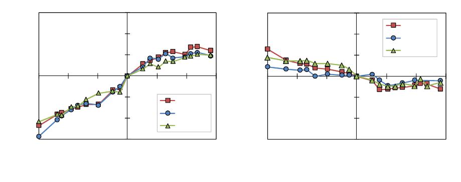
from 0% to 0.5%; a further increase in the magnitude of applied strain results in a saturation in
the change of both electron and hole effective mobilities. Under compressive strain the effective
electron mobility decreases by 50% while that of holes increases by 20% monotonously as the
strain increases from 0% to -1.2%. The effect of strain on mobility is more pronounced for n-
channel poly-Si TFTs especially under compression.
In single crystalline silicon MOS devices, the electron and hole mobilities under uniaxial
strain have been extensively studied [8, 11-15] because of the significance of strained silicon
technology to improve performance of nanoscale silicon MOS devices. It was noted that strain-
induced band splitting affects carrier repopulation and suppresses the scattering of carriers.
Furthermore the carrier transport is also affected by a change in the carrier effective mass which
is induced by strain. As a result the mobility of electrons is enhanced under uniaxial tensile
strain while reduced under uniaxial compressive strain parallel to the channel; however, these
trends tend to be reversed for holes. The electron mobility saturation at higher level of tensile
strain is due to the saturation of band splitting effects [13]. Since the poly-Si thin film material,
particularly when it is prepared by the SLS method, is composed by large crystalline silicon
grains, we can infer that the change of electron and hole mobilities under strain in our
experiment is related to the aforementioned effects present in single crystalline silicon devices.
0.4
0.6
0.8
1
1.2
1.4
1.6
-1.2 -0.8 -0.4 0.0 0.4 0.8 1.2
µ/µ
o
Strain (%)
n_W16L8
n_W32L8
n_W64L8
(a)
0.4
0.6
0.8
1
1.2
1.4
1.6
-1.2 -0.8 -0.4 0.0 0.4 0.8 1.2
µ/µ
o
Strain (%)
p_W16L8
p_W32L8
p_W64L8
(b)
Figure 4. Normalized mobility as a function of strain for (a) n-channel and (b) p-channel poly-Si
TFT
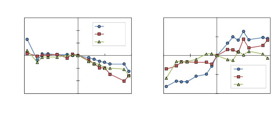
As shown in figure 5(a), in p-channel TFTs the normalized threshold voltage decreases
under tensile and almost remains unchanged under compressive strain; however, for n-channel
TFTs the effect of strain on the change of threshold voltage is not obvious. Figure 5(b) shows the
normalized subthreshold slope of p-channel TFTs which increases under tensile while decreases
under compressive strain. It is interesting to note that this phenomenon is more pronounced in
smaller channel length devices. No obvious trend was found for that of n-channel TFTs under
strain. All the tested poly-Si TFTs remained functional under the applied strain that ranged from
-1.2% to 1.1%.
0.7
0.8
0.9
1
1.1
1.2
1.3
-1.0 -0.5 0.0 0.5 1.0
V
th (V)
Strain (%)
p_W16L4
p_W16L8
p_W32L8
(a)
0.6
0.8
1
1.2
1.4
-1.0 -0.5 0.0 0.5 1.0
S/S
O
Strain (%)
p_W16L4
p_W16L8
p_W32L8
(b)
Figure 5. Normalized (a) threshold voltage and (b) subthreshold slope of p-channel poly-Si TFT
as a function of applied strain
CONCLUSIONS
We fabricated n-channel and p-channel poly-Si TFTs on stainless steel foil and investigated
the effects of uniaxial strain on the electrical characteristics of these devices. It was observed that
the effective electron mobility increased under tensile and decreased under compressive strain
while that of holes behaved in an opposite way. The effect of strain on mobility is more
pronounced in n-channel poly-Si TFTs especially under compression. For p-channel poly-Si
TFTs the normalized threshold voltage decreased under tensile strain but remained unchanged
under compressive strain, and the normalized subthreshold slope increased under tensile strain
but decreased under compressive strain. No obvious trends were observed for the threshold
voltage and the subthreshold slope of n-channel poly-Si TFTs either under tensile or compressive
strain. The off current for both n- and p-channel poly-Si TFTs decreased under tensile while
increased under compressive strain. The change in the poly-Si TFT device characteristics caused
by the mechanical strain should be taken into account during the design of flexible electronic
circuits when based on this technology. It is important to note that all TFTs remained functional
under the entire range of applied strain from -1.2% to 1.1% with no obvious physical damage
observed. This shows that the poly-Si TFT technology on stainless steel foil is suitable for
flexible electronics application.
ACKNOWLEDGMENT
The authors would like to acknowledge the financial support of this work from ARL, NASA,
The FlexTech Alliance and the Sherman Fairchild Foundation. The authors also wish to thank
Dr. Tolis Voutsas from Sharp Laboratories of America for his assistance with the SLS
crystallization process.
REFERENCES
[1] M. N. Troccoli, A. J. Roudbari, T. K. Chuang, and M. K. Hatalis, "Polysilicon TFT
circuits on flexible stainless steel foils," Solid State Electronics, vol. 50, pp. 1080-1087,
2006.
[2] T. K. Chuang, M. Troccoli, P. C. Kuo, A. Jamshidi-Roudbari, M. K. Hatalis, I. Biaggio,
and A. T. Voutsas, "Top-emitting 230 dots/ in. active-matrix polymer light-emitting
diode displays on flexible metal foil substrates," Applied Physics Letters, vol. 90, p.
151114, 2007.
[3] H. Gleskova, S. Wagner, W. Soboyejo, and Z. Suo, "Electrical response of amorphous
silicon thin-film transistors under mechanical strain," Journal of Applied Physics, vol. 92,
p. 6224, 2002.
[4] S. H. Won, J. K. Chung, C. B. Lee, H. C. Nam, J. H. Hur, and J. Jang, "Effect of
Mechanical and Electrical Stresses on the Performance of an a-Si: H TFT on Plastic
Substrate," Journal of The Electrochemical Society, vol. 151, p. G167, 2004.
[5] T. Sekitani, S. Iba, Y. Kato, Y. Noguchi, T. Sakurai, and T. Someya, "Submillimeter
radius bendable organic field-effect transistors," Journal of Non-Crystalline Solids, vol.
352, pp. 1769-1773, 2006.
[6] P. C. Kuo, A. Jamshidi-Roudbari, and M. Hatalis, "Effect of mechanical strain on
mobility of polycrystalline silicon thin-film transistors fabricated on stainless steel foil,"
Applied Physics Letters, vol. 91, p. 243507, 2007.
[7] A. T. Voutsas, A. Limanov, and J. S. Im, "Effect of process parameters on the structural
characteristics of laterally grown, laser-annealed polycrystalline silicon films," Journal of
Applied Physics, vol. 94, p. 7445, 2003.
[8] Y. Sun, S. E. Thompson, and T. Nishida, "Physics of strain effects in semiconductors and
metal-oxide-semiconductor field-effect transistors," Journal of Applied Physics, vol. 101,
p. 104503, 2007.
[9] T. J. Wang, C. H. Ko, S. J. Chang, S. L. Wu, T. M. Kuan, and W. C. Lee, "The Effects of
Mechanical Uniaxial Stress on Junction Leakage in Nanoscale CMOSFETs," Electron
Devices, IEEE Transactions on, vol. 55, pp. 572-577, 2008.
[10] K. R. Olasupo and M. K. Hatalis, "Leakage current mechanism in sub-micron polysilicon
thin-filmtransistors," Electron Devices, IEEE Transactions on, vol. 43, pp. 1218-1223,
1996.
[11] H. Irie, K. Kita, K. Kyuno, and A. Toriumi, "In-plane mobility anisotropy and
universality under uni-axial strains in nand p-MOS inversion layers on (100),[110], and
(111) Si," IEDM Technical Digest, pp. 225-228, 2004.
[12] K. Uchida, R. Zednik, C. H. Lu, H. Jagannathan, J. Mc Vittie, P. C. McLntyre, and Y.
Nishi, "Experimental study of biaxial and uniaxial strain effects on carrier mobility in
bulk and ultrathin body SOI MOSFETs," IEDM Technical Digest pp. 229-232, 2004.
[13] K. Uchida, T. Krishnamohan, K. C. Saraswat, and Y. Nishi, "Physical mechanisms of
electron mobility enhancement in uniaxial stressed MOSFETs and impact of uniaxial
stress engineering in ballistic regime," IEDM Technical Digest, pp. 120-132, 2005.
[14] E. X. Wang, P. Matagne, L. Shifren, B. Obradovic, R. Kotlyar, S. Cea, M. Stettler, and
M. D. Giles, "Physics of Hole Transport in Strained Silicon MOSFET Inversion Layers,"
Electron Devices, IEEE Transactions on, vol. 53, pp. 1840-1851, 2006.
[15] S. Kobayashi, M. Saitoh, Y. Nakabayashi, and K. Uchida, "Experimental study of
uniaxial stress effects on Coulomb-limited mobility in p-type metal-oxide-semiconductor
field-effect transistors," Applied Physics Letters, vol. 91, p. 203506, 2007
