
Selective Deposition of C-axis Oriented Pb
5
Ge
3
O
11
on the Patterned High k
Gate Oxide by MOCVD Processes
Tingkai Li,
Sheng Teng Hsu, Bruce Ulrich, Dave Evans
Sharp Laboratory of America, Inc. 5700 NW Pacific Rim Blvd. Camas, WA 98607
ABSTRACT
For the high density FeRAM applications, the integration process-induces damages such as
etching damage that degrades the properties of FRAM devices and the high surface roughness of
ferroelectric thin film that results in the difficulty for alignment are critical issues. In order to
solve these problems, selective deposition process is developed to simplify the integration
processes and improve the properties of FeRAM memory devices. Based on the differential
deposition rates of ferroelectric materials on high-k oxide and silicon dioxide, we can selectively
deposit a c-axis oriented PGO thin film on the patterned high-k oxide such as ZrO
x
(x=0-2),
HfO
x
(x=0-2), TiO
2
, and their mixtures other than on SiO
2
. By patterning the high-k dielectric,
the PGO deposition is limited to just the preferred pattern high-k area. SEM, EDX and x-ray
measurements further confirm that the c-axis oriented PGO thin films are selectively deposited
on the high-k gate oxide other than on the field SiO
2
including alignment mark area, which will
eliminate the roughness problem for the alignments. Also the etching damage is eliminated
since there is no need to etch the PGO film, which improved the properties of FeRAM devices.
INTRODUCTION
The remanent-polarization states of ferroelectric capacitors have long been of interest for
nonvolatile storage of digital data [1-5]. The recent approach to ferroelectric memories has been
to integrate the ferroelectric memory capacitor into a random access memory circuit on an
integrated circuit to convert semiconductor RAMs to a nonvolatile form. Most of the studies on
Ferroelectric Random Access Memories (FeRAM) have been concentrated on the memory
structure with one transistor and one capacitor (1T1C), and one transistor (1T) memory devices
with MFMIS (Metal/Ferroelectrics/Metal/Insulator/Silicon) and MFIS structures have also been
fabricated recently [6-10]. However, for smaller devices and higher density application of
FeRAM devices, the ferroelectric thin film are related to the integration process induced
damages, which degrades the working function of FeRAM devices [11]. Therefore, we
improved the integration processes including damascene structure, selective deposition and
chemical mechanical planarization (CMP). For 1T memory devices, C-axis oriented Pb
5
Ge
3
O
11
thin films showed the very good ferroelectric and electrical properties for the 1T-memory device
applications. Extremely high c-axis oriented PGO thin films can be deposited on high k gate
oxides, and the working 1T-memory devices with PGO MFIS memory cell have also been
fabricated.
In this paper, we proposed the selective deposition technologies for c-axis oriented PGO thin
films on high k gate oxides including ZrO
X
(x=0-2), HfO
X
(x=0-2), TiO
2
, Al
2
O
3
, La
2
O
3
and their
mixtures to simplify the integration processes and improve the properties of PGO MFIS
transistor ferroelectric memory devices. There is no need to etch ferroelectric material; as a
Mat. Res. Soc. Symp. Proc. Vol. 784 © 2004 Materials Research Society C9.9.1/E9.9.1
result the etching induced damage is avoided. Due to the selective deposition of PGO on
patterned high k gate oxide other than on field oxide, the alignment problem is also solved.
2. THE EXPERIMENTAL METHODS AND RESULTS
P type Si wafers were used as the substrates of PGO MFIS one-transistor devices. The
integration processes including STI, polysilicon or nitride gate replacement for damascene
structures, high k gate oxide deposition, pattern and etching, MOCVD selective deposition,
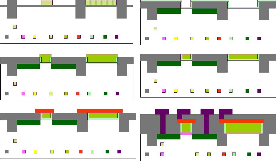
CMP etc. have been used for the one-transistor memory device, as shown in Fig. 1a - 1f. The
detail integration processes are as follows.
Fig.1a shows the processes including threshold adjustment ion implantation, grow gate oxide,
CVD nitride, STI photoresist, CVD oxide, CMP oxide stopped at nitride, photoresist, and
etch Nitride.
Fig.1b shows the processes including source and drain ion implantation, CVD oxide. CMP
oxide
stopped at nitride wet etches nitride and gate oxide, and deposition of high k gate oxide.
Fig.1c shows the processes including pattern and etch high k oxides (such as HfO
2
) stopped at
field oxide (SiO
2
), and selective deposition of ferroelectric thin film (such as PGO) on
high k gate oxides (such as HfO
2
).
Fig.1d shows the process of CMP ferroelectric thin film (such as PGO) stopped at oxide.
Fig.1e shows deposition of top electrodes and patterned the electrodes.
Fig.1f shows the final device structure including etching contact holes and metallization.
Oxide BE Resist Poly FE TE TiO2 N+ Metal
Nitride
A
Oxide BE Resist Poly FE TE HfO2 N+ Metal
Nitride
B
Oxide BE Resist Poly FE TE HfO2 N+ Metal
Nitride
C
Oxide BE Resist Poly FE TE HfO2 N+ Metal
Nitride
D
Oxide BE Resist Poly FE TE HfO
2
N+ Metal
Nitride
E
Oxide high k gate oxide FE Poly TE HfO2 N+ Metal
Nitride
F
Fig. 1 The integration processes for the MFIS 1T memory devices
C9.9.2
/E9.9.2
The etching and pattern high k gate oxides is a critical process for the PGO MFIS 1T
transistor memory device applications, as shown in Figure 1c. We developed the following
processes to pattern HfO
2
: In the first step, we deposited Hf metal on SiO
2
, then patterned Hf
metal, and finally annealed Hf metal at forming gas or oxygen atmosphere to transfer the Hf
metal into HfO
2
. Figure 2 shows the patterned HfO
2
using dry etching processes.
Fig. 2 The patterned Hf thin films using dry etching processes
According to experimental results, MOCVD PGO thin films deposited on high-k gate oxide
and SiO2 have different deposition rates and different microstructures, as shown in table 1.
Because the huge difference between the deposition rates of PGO grown on HfO
2
to PGO grown
Table 1. The deposition rates of PGO grown on HfO
2
and SiO
2
Deposition rates (nm/hour) Crystallization
PGO on HfO
2
200 - 300 Oriented crystallized film
PGO on SiO
2
1 - 5 Amorphous film
on SiO
2
, PGO thin films can be selectively deposited on HfO
2
other than on field oxide of SiO
2
.
The following is the detail of selective MOCVD processes. [Pb(thd)
2
] and [Ge(ETO)
4
] with a
molar ratio of 5 – 5.5:3
were dissolved in a mixed solvent of butyl ether or tetrahydrofuran,
isopropanol and tetraglyme in the molar ratio of 8:2:1. The precursor solutions had a
concentration of 0.1 M/L of PGO. The solution was injected into a vaporizer at temperature in
the range of 150 – 240ºC by a pump at a rate of 0.02 – 0.2 ml/min to form precursor gases. The
feed line was kept at 150 - 245ºC.
Substrate: patterned HfO
2
and field SiO
2
Deposition temperatures: 500 - 520ºC, Deposition pressure: 1 - 10 torr
Oxygen partial pressures: 30 – 50%.
Vaporizer temperature: 180 - 200ºC
Vaporizer pressure: 30 - 50 torr.
Solution delivery rates: 0.02 - 0.2 ml/min
Deposition time: 1 - 3 hours depending on film thickness
Annealing temperatures: 500 - 560ºC, Annealing time: 5 – 30 minutes at O
2
HfO2
C9.9.3/E9.9.3
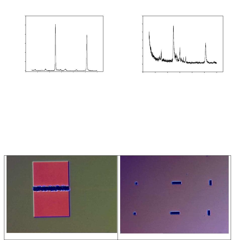
Fig. 3 shows the x-ray pattern of PGO thin film deposited on HfO
2
gate oxide of test wafer. As
is shown in the figure, the extremely high c-axis oriented PGO thin film is obtained. Fig. 4
shows the x-ray pattern of PGO thin film selective deposited on patterned HfO
2
device wafers.
The x-ray pattern confirmed that the selective deposited thin films on patterned HfO
2
device
wafer is c-axis oriented PGO thin film.
2 Theta
0 102030405060
Counts/S
0
2000
4000
6000
8000
10000
12000
001
002
003
006
004
005
Fig. 3 X-ray pattern of PGO thin films
deposited on HfO
2
test wafer
2 Theta
0 102030405060
Counts/S
-50
0
50
100
150
200
250
300
001
002
003
006
004
005
Fig. 4 X-ray pattern of PGO thin films
deposited on patterned HfO
2
device wafer
Fig. 5A and 5B show the microphotographs of selective deposition of PGO thin films on HfO
2
.
These figures confirmed PGO thin films have been selective deposited on HfO
2
gate oxide other
than on SiO
2
. Fig. 6 shows the microstructure of PGO thin film deposited on HfO
2
substrate.
The grain size of PGO thin films deposited on HfO2 is about 0.3 µm.
A
B
Fig. 5 The microphotographs for PGO selective deposition on HfO
2
gate oxide
Using MOCVD PGO selective deposition technologies, damascene structure and CMP
processes, the 1T MFIS memory device have been fabricated. Fig. 7 shows the drain current (I
D
)
versus drain voltage (V
D
) with various gate voltages of 10 x10 µm 1T memory device. The
C9.9.4
/E9.9.4
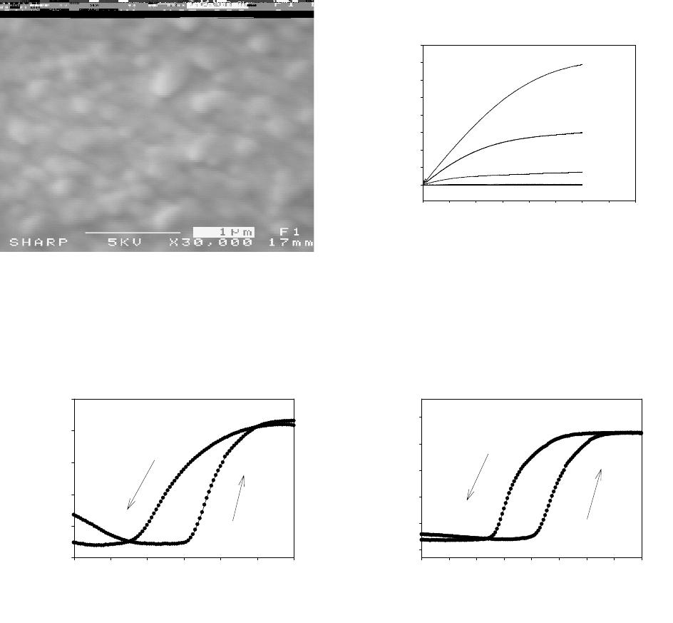
drain current (I
D
) increased with increasing drain voltage (V
D
). The drain current (I
D
) also
increased with increasing gate voltage (V
G
). The behavior showed a typical working function of
a transistor device. Fig. 8a and 8b shows the I
D
– V
G
curves of 1T MFIS memory devices with
device size of 5 x10 µm and 10 x10 µm respectively. The memory window is about 2V, the
drain current at “off” state with V
D
of 0.1 V is about 2 x 10
-12
A, and the drain current at “on”
state with V
D
of 0.1 V is about 4 x 10
-8
A. The ratio of “on/off” states is about 4 orders, which
is enough for memory device applications.
Fig. 6 The microstructure of PGO thin film
deposited on HfO2 substrate
Fig. 7 The drain current (I
D
) versus drain
voltage (V
D
) with various gate voltages
A. Device size: 5 x10 µm
B. . Device size: 10 x10 µm
Fig. 8 The I
D
– V
G
curves of 1T MFIS memory devices with device size
of 5 x10 µm and 10 x10 µm
Drain voltage (V
D
)
0.0 0.5 1.0 1.5 2.0 2.5 3.0 3.5 4.0
Drain Current I
D
(A)
0
2.0x10
-5
4.0x10
-5
6.0x10
-5
8.0x10
-5
10
-4
1.2x10
-4
1.4x10
-4
1.6x10
-4
V
g
: 3 V
V
g
: 4 V
V
g
: 5.0 V
V
g
: 1, 2 V
Gate voltage (V
G
)
-3-2-1012345
Drain Current I
D
(A)
10
-12
10
-11
10
-10
10
-9
10
-8
10
-7
From -5V to +5V
From +5V to -5V
Gate voltage (V
G
)
-1012345
Drain Current I
D
(A)
10
-12
10
-11
10
-10
10
-9
10
-8
10
-7
From -5V to +5V
From +5V to -5V
C9.9.5
/E9.9.5
MFIS (Metal/Ferroelectrics/Insulator/Silicon) transistor ferroelectric memory devices have been
fabricated. For the small device and high density 1T FeRAM device applications, the selective
deposition processes have been developed to simplify the integration processes and improve the
properties of MFIS transistor ferroelectric memory devices. Based on the different deposition
rates of ferroelectric materials on high-k oxide and silicon dioxide, we can selectively deposit a
c-axis oriented PGO thin film on the patterned high-k oxide such as ZrO
x
(x=0-2), HfO
x
(x=0-
2), TiO
2
, and their mixtures other than on SiO
2
. By patterning the high-k dielectric, the PGO
deposition is limited to just the preferred pattern high-k area. SEM, EDX and x-ray
measurements further confirmed that the c-axis oriented PGO thin films were selectively
deposited on the high-k gate oxide other than on the field SiO
2
. The etching damage is
eliminated since there is no need to etch the PGO film. The properties of 1T MFIS memory
devices are also improved.
REFERENCES
1. Ramtron Corporation (Colorado Springs, CO) started introducing its 4Kbit, 8Kbit, and
16Kbit FRAMs in 1988.
2. S.B. Desu and Tingkai. Li, Mat. Sci. and Eng. B 34, L4-L8 (1995).
3. C.A. Paz de Araujo, J. D. Cuchiaro, L.D. McMillan, M.C. Scott & J.F. Scott, Nature, 374,
13, 627-629 (1995).
4. Tingkai Li, Y.F. Zhu, S.B. Desu, C.H. Peng, and N. Masaya, Appl. Phys. Letters 68 (5), 616
(1997).
5. Tingkai Li, F.Y. Zhang and S.T. Hsu, Appl. Phys. Lett. 74 (2) 296 (1999).
6. S. Imada, S. Shouriki, E. Tokumitsu, and H. Ishiwara, Jpn. J. Appl. Phys. 37, 6497 (1998).
7. Tingkai Li, S. T. Hsu, B. Ulrich, H. Ying, L. Stecker, D. Evans, Y. Ono, J. S. Maa, J. J. Lee
Appl. Phys. Lett. 79 (11) 1661 (2001).
8. Tingkai Li, S. T. Hsu, B. Ulrich, L. Stecker, D. Evans, J. J. Lee, IEEE Electron Device
Letters, vol. 23, No. 6, 339 (2002).
9. E. Tokumitsu, G. Fujii and H. Ishiwara, Jpn. J. Appl. Phys. vol. 39, 2125 (2000).
10. Tingkai Li, S. T. Hsu, B. Ulrich, D. Evans, IEEE Transactions on Electron Devices, vol. 50,
No.11, 2280 (2003)
11. Tingkai Li, S. T. Hsu, B. Ulrich, L. Stecker, D. Evans, Jpn. J. Appl. Phys. Vol.41, 6890
(2002).
C9.9.6/E9.9.6
3. SUMMARY
