Mater. Res. Soc. Symp. Proc. Vol. 1577 © 2013 Materials Research Society
DOI: 1 557/op 0130.1 l.2 .
High Mobility IGZO/ITO Double-layered Transparent Composite Electrode: A Thermal
Stability Study
Aritra Dhar
1
and T. L. Alford
1,2
1
Department of Chemistry and Biochemistry,
2
School for Engineering of Matter, Transport, and Energy,
Arizona State University, AZ 85287, U.S.A.
ABSTRACT
The fabrication of a thin film optoelectronic device involves the exposure of the transparent
conductive oxide (TCO) to a high process temperature. Indium gallium zinc oxide (InGaZnO
4
or
IGZO) is a well known TCO with high optical transparency, moderate conductivity and high
mobility. However, its electrical properties deteriorate after subsequent high temperature
processes in air atmosphere. On the other hand indium tin oxide (ITO) has higher conductivity
than IGZO and better thermal stability. Therefore, IGZO/ITO bilayers have been deposited on
glass by radio frequency magnetron sputtering at room temperature and subsequently annealed at
high temperatures in order to study their thermal stability. In the present work, a-IGZO layers
with a thickness ranging from 10 nm to 100 nm were deposited over a 50 nm thick ITO layer.
Results are compared with those from a single IGZO layered thin film without the ITO bottom
layer. The structural, optical and electrical properties of the multilayers are studied with the use
of scanning electron microscopy, UV–Vis spectroscopy and Hall measurement. An IGZO
optimal thickness of 50 nm is found to improve the bilayer thermal stability at temperatures upto
400 °C keeping good opto-electrical properties. The sheet resistance for the optimized
IGZO/ITO composite films is about 22 Ohm/sq, and the transmittance in the visible range is
about 90%. The composite shows an excellent mobility above 40 cm
2
/V-s and thus can be
potentially applied as channel layer in thin film transistors (TFTs)
INTRODUCTION
Transparent conducting oxides (TCO) have been widely used for various optoelectronic
applications such as solar cells, [1] flat panel displays [2], gas sensors [3] and organic light
emitting diodes [4]. TCO thin films are critical for solar cell devices since they constitute a
essential part in the future generations of photovoltaic (PV) devices [5]. The most important
criteria for a TCO is to have high visible transparency and good electric conductivity. Also, low
cost abundance, non toxicity, and simple fabrication methods at an industrial scale are other
important characteristics to be considered for the selection of a TCO electrode for photovoltaic
applications [6-10]. However, apart from these conventional characteristics, processing of PV
devices requires high thermal and chemical stability, surface electrochemical properties and
room temperature fabrication. For this reason, the research for new materials or various
composites had been extensively studied to improve the performance and efficiency of the TCO
662
thin films. ITO is the most common and widely used TCO which has good properties in terms of
high transparency and conductivity[8-13]. The advantage of ITO is that it can be easily
fabricated at room temperature by magnetron sputtering [5] on both glass and plastic substrates.
However, it looses its good electrical conductivity on thermal annealing at 350 °C in air
atmosphere [6]. On the other hand amorphous Indium gallium zinc oxide (a-IGZO) is another
potential TCO material which can also be easily deposited at ambient temperature by RF
magnetron sputtering. However the as-deposited IGZO samples have poorer electrical
conductivity, but show a high improvement in conductivity when annealed at high (over 300 °C)
temperatures. On the basis of these rationalities, the main objective of the present research work
is focused on the development of a double-layered transparent composite IGZO/ITO electrode.
The bilayer thin films are deposited without direct substrate heating, and expected to exhibit
good electrical properties even when annealed at higher temperature. The thermal stability of the
thin film had been studied and the effect of annealing in various environments had been
discussed in details.
EXPERIMENTAL DETAILS
IGZO/ITO double-layered transparent composite electrodes were deposited on 2 mm thick
soda-lime glass substrates at room temperature by two sequential RF magnetron sputtering
processes of ITO and InGaZnO
4
targets. The In and Ga content is about 25 at. % and 35 at. %
respectively, in the mixed oxide. The base pressure of the sputter system prior to each deposition
was approximately 1x10
−7
Torr. The deposition was performed at a pressure of 10 mTorr for ITO
and 20 mTorr for IGZO in pure Ar gas (99.999%). The depositional parameters for sputtering of
both the individual metal oxides had been optimized prior to the bilayer deposition. The ITO and
IGZO layers were deposited using an rf power of 100 W and 150 W, respectively. The target-to-
substrate distance was maintained at 6 cm for all the depositions. The thickness of the ITO and
IGZO layers were measured using optical ellipsometry. The bottom ITO layer was kept constant
at 50 nm while the top IGZO layer was varied between 10 nm to 100 nm. Post deposition, the
IGZO/ITO bilayers were annealed at 100 °C, 200 °C, 300 °C and 400 °C in a quartz tube furnace
in air atmosphere for 3 hours in order to study their thermal stability. Optical transmittance of the
multilayers were measured using an Ocean Optics double channel spectrometer (model DS200)
in the wavelength range of 300–800 nm with an air reference for transmittance. Tungsten
halogen and deuterium lamps were used as sources for visible and UV light, respectively. Hall
measurements were done using a HMS3000 instrument. Electrical resistivity, Hall mobility, and
carrier concentration of the films were measured by means of the Van der Pauw method. A
magnetic field of 0.98 T was applied perpendicular to the sample surface.
RESULTS
IGZO and ITO thin films exhibit a considerably different behavior in their electrical
properties when they are exposed at high temperatures (Fig. 1). The as-deposited has lower
electrical resistivity at room temperature than ITO and it became better on thermal annealing at
above 300
o
C. However the electrical resistivity in IGZO is seen to increase with annealing
temperature and showed significant rise after 300
o
C. However, in both the materials shallow
donor levels present near the conduction band results in forming Drude-like absorption in far
infrared wavelengths [7] leaving the material transparent in the visible region (400–800 nm). For
IGZO films, this donor levels come from oxygen intrinsic defects and impurity doping.

Now, it is seen that ITO is stable under high temperature processes. On the other hand, IGZO
layers deposited at room temperature can show different behavior in their conductivity
depending on the post-deposition annealing temperature and also on the annealing environment.
The variations are attributed mainly due to change in their carrier concentration because of the
creation or annihilation of donor oxygen vacancies and changes in the effective doping of In and
Ga onto Zn lattice sites [7]. After heating at 300 °C in air the conductivity increases mainly due
to carrier concentration increase. But on annealing above this temperature in air atmosphere,
there is a sharp decline in the conductivity due to the isolation of interstitial metal atoms in grain
boundaries and the annihilation of oxygen vacancies. However, the as-deposited IGZO/ITO
bilayer is seen to have lower sheet resistance and exhibit little increase in electrical resistance on
thermal annealing above 300
o
C in air atmosphere.
Fig.1 Sheet resistance vs. annealing temperature in air for 50 nm thick individual ITO, IGZO
thin films and IGZO/ITO composites.
Fig. 2 shows the effect of increasing IGZO top layer on the electrical properties of IGZO/ITO
bilayer where both resistivity and sheet resistance shows a sharp decrease on addition of a 10
nm of IGZO layer. The effective resistivity of the bilayer continues to decrease with increase in
IGZO thickness. The effective resistivity of the bilyaer is seen to drop down to almost 1 order of
magnitude from the initial resitivity of as-deposited ITO sample. A 50 nm thick as-deposited
IGZO thin films shows a resistivity and sheet resistance of 9.7 x 10
-3
ohm.cm and 1.07 x 10
3
ohm/sq respectively at room temperature.

Fig. 2 Effective resistivity and sheet resistance of IGZO/ITO multilayer films
Figure 3 shows the change in carrier concentration and hall mobility as a function of IGZO
thickness for IGZO/ITO bilayer. The plot indicates that both carrier concentration and hall
mobility increase sharply with the addition of IGZO layer and continues to increase with the
addition of thicker IGZO layer. The carrier concentration of the bilayer has increased from 1.3 x
10
19
to 10.2 x 10
20
cm
-3
upon increase of IGZO thickness from 10 to 100 nm. Also the hall
mobility of the bilayer increased to a maximum of 44 cm
2
/V-s from 23 cm
2
/V-s in case of only
ITO thin films.
Fig. 3 Hall mobility and Carrier concentrations of IGZO/ITO multilayer films.
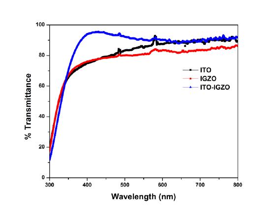
Figures 4 show optical transmittance spectra for individual oxides and IGZO/ITO multilayer on
glass substrate. The maximum optical transmittance of the pure single-layer ITO and IGZO thin
films are about 87% and 81% respectively, in the visible region. The transmittance was seen to
increase in the bilayer than the individual oxides.
Fig. 4 Optical transmittance spectra for individual oxides and IGZO/ITO multilayer on glass
substrate
For the IGZO/ITO bilayer electrodes in Fig. 4, increasing the IGZO thickness to 50 nm shows
high transmittance. However, a further increase thereafter results in poorer average optical
transmittance. Preliminary results suggest that the optimized bilayer electrode doesn’t exhibit
any significant decrease in optical transmittance when annealed upto 400
o
C for 24 hours which
suggest the high thermal stability of the composite.
CONCLUSION
Novel IGZO/ITO bilayers transparent composite electrodes were successfully deposited on
glass substrates by RF magnetron sputtering at room temperature. An ITO layer is found to be
able to provide thermal stability in terms of electrical conductivity at temperatures over 300 °C
in air atmosphere. However the IGZO/ITO bilayer showed better electrical conductivity both as-
deposited and post-annealed than the individual thin films. The strongly stable structure of ITO
prevents the oxygen diffusion during the annealing, therefore it avoids the oxygen vacancy
annihilation in IGZO, keeping its good electrical properties. The IGZO optimal thickness was
found to be 50 nm, thinner layers do not provide as good protection, however thicker layers
deteriorate the electrode series resistance.
.
ACKNOWLEDGMENTS
This work was partially supported by the National Science Foundation (C. Ying, Grant No.
DMR-0902277) to whom the authors are greatly indebted.
REFERENCES
[1] E. Harlev, T. Gulakhmedova, I. Rubinovich, and G. Aizenshtein, Adv. Mater. 8, 994,
(1996).
[2] C. Guillén, J. Herrero , Thin Solid Films 520 (2011) 1
[3] G. Gustafsson, Y. Cao, G.M. Treacy, F. Klavetter, N. Colaneri, and A. J. Heeger,
Nature 357, 477, (1992).
[4] C. G. Granqvist, Appl. Phys. A 52, 83, (1991).
[5] H. C. Lee, and O. O. Park, Vacuum 75, 275, (2004).
[6] A. E. Hichou, A. Kachouane, J. L. Bubendorff, M. Addou, J. Ebothe, M. Troyon, and
A. Bougrine, Thin Solid Films 458, 263, (2004).
[7] J. Montero, C. Guillén, J. Herrero, Thin Solid Films 519, 7564,(2011).
[8] D. C. Look, Semicond. Sci. Technol. 20, S55, (2005).
[9] A. Dhar and T. L. Alford, J. Appl. Phys. 112, 103113 (2012).
[10] A. Indluru and T. L. Alford, J. Appl. Phys. 103, 013708, (2008).
[11] S. W. Chen, and C. H. Koo, Mater. Lett. 61, 4097, (2007).
[12] K. H. Choi, J. Y. Kim, Y. S. Lee, and H. J. Kim, Thin Solid Films 341, 152, (1999).
[13] M. K. Sinha, S. K. Mukherjee, B. Pathak, R. K. Paul, P. K. Barhai, Thin Solid Films
515, 1753, (2006).
[14] M. Gadre and T. L. Alford, Appl. Phys. Lett. 99, 051901 (2011)
