MRS Internet Journal of Nitride Semiconductor Research
http://journals.cambridge.org/MIJ
Additional services for MRS Internet Journal of Nitride Semiconductor Research:
Email alerts: Click here
Subscriptions: Click here
Commercial reprints: Click here
Terms of use : Click here
Characteristic of InGaN/GaN Laser Diode Grown by a Multi-Wafer MOCVD
System
Y. Park, B.j. Kim, J. W. Lee, O. H. Nam, C. Sone, H. Park, Oh Eunsoon, H. Shin, S. Chae, J. Cho, Ig-Hyeon Kim, J.S. Khim, S.
Cho and T.I. Kim
MRS Internet Journal of Nitride Semiconductor Research / Volume 4 / Issue 01 / January 1999
DOI: 10.1557/S1092578300000570, Published online: 13 June 2014
Link to this article: http://journals.cambridge.org/abstract_S1092578300000570
How to cite this article:
Y. Park, B.j. Kim, J. W. Lee, O. H. Nam, C. Sone, H. Park, Oh Eunsoon, H. Shin, S. Chae, J. Cho, Ig-Hyeon Kim, J.S. Khim, S.
Cho and T.I. Kim (1999). Characteristic of InGaN/GaN Laser Diode Grown by a Multi-Wafer MOCVD System . MRS Internet
Journal of Nitride Semiconductor Research, 4, pp e1 doi:10.1557/S1092578300000570
Request Permissions : Click here
Downloaded from http://journals.cambridge.org/MIJ, IP address: 134.129.120.3 on 08 Jun 2015

MRS Internet J. Nitride Semicond. Res. 4, 1 (1999). 1
© 1999 The Materials Research Society
M
RS
Internet Journal ResearchNitride Semiconductor
Characteristic of InGaN/GaN Laser Diode Grown by a
Multi-Wafer MOCVD System
Y. Park
1
, B. J. Kim
1
, J. W. Lee
1
, O. H. Nam
1
, C. Sone
1
, H. Park
1
, Eunsoon Oh
1
, H. Shin
1
, S. Chae
1
,
J. Cho
1
, Ig-Hyeon Kim
1
, J.S. Khim
1
, S. Cho
1
and T.I. Kim
1
1
Samsung Advanced Institute of Technology,
(Received Wednesday, January 6, 1999; accepted Tuesday, January 19, 1999)
InGaN/GaN multi-quantum well (MQW) laser diodes (LDs) were grown on c-plane sapphire
substrates using a multi-wafer MOCVD system. The threshold current for pulsed lasing was 1.6 A
for a gain-guided laser diode with a stripe of 10 x 800
µ
m
2
. The threshold current density was 20.3
kA cm
-2
and the threshold voltage was 16.5 V. The optical power ratio of transverse electric mode
to transverse magnetic mode was found to be greater than 50. The characteristic temperature
measured from the plot of threshold current versus measurement temperature was between 130 and
150K.
1 Introduction
Nitride semiconductor short wavelength laser diodes
(LD) have attracted much attention as a light source for
the optical data storage. Since Nichia Co. reported
pulsed lasing in an InGaN multi-quantum well (MQW)
LD in the end of 1995, [1] significant progress has been
made in the development of blue LD’s. Nakamura et al.
has already demonstrated a blue LD with lifetime in
excess of 10,000 hrs. [2] Although Nichia’s conspicu-
ous successes have stimulated the nitride research soci-
ety during the last three years, until recently a limited
number of research groups in the United States and
Japan reported continuous wave [3] [4] [5] or pulsed
lasing. [6] [7] [8] [9] In this paper, we report InGaN/
GaN MQW LD operated under pulsed conditions.
2 Experiment
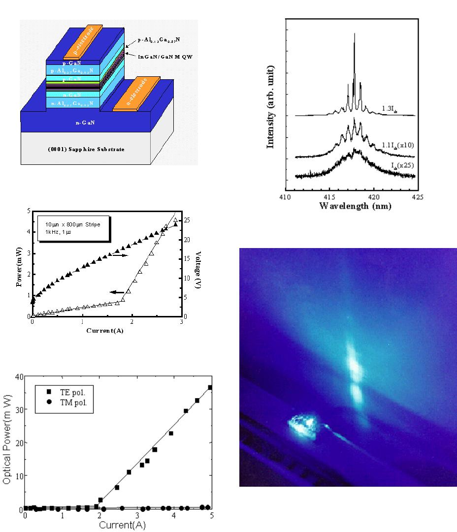
The LD structure shown in Figure 1 was grown on a c-
plane sapphire substrate using a multi-wafer MOCVD
system into which three 2” wafers can be loaded in a
time. To our knowledge, this is the first report on
InGaN/GaN MQW LD grown by a mass production
scale MOCVD reactor in the open literature. TMGa,
TMIn, TMAl, Cp
2
Mg, NH
3
, and SiH
4
were used as
material sources for the structure growth. The reactor
pressure was maintained at 100 torr during the growth.
In order to form gain guided LD’s the structure was
etched using chemically assisted ion beam etching
(CAIBE) until the n-type GaN layer was exposed. A Pd/
Au contact was formed onto the p-type GaN, and a Ti/Al
contact onto the n-GaN. The laser facets were formed
by CAIBE. No mirror coating was employed on the
facet surface. Fabricated LDs were measured under
pulsed current conditions with pulse widths ranging
from 100 ns to 1
µ
sec at 1 kHz.
3 Results
Figure 2, Figure 3, Figure 4, Figure 5 show typical fea-
tures proving that the diodes lased. Figure 2 shows L-I-
V characteristics of one of the LDs with a stripe of 10
µ
m x 800
µ
m. The lowest threshold current was found
to be 1.6 A, corresponding to a threshold current density
of 20.3 kA cm
-2
. The threshold voltage of the device at
the threshold current was 16.5 V. Figure 3 shows the
polarized light output intensity as a function of current
for another LD, whic hwas measured under a pulse con-
dition of 200 ns width at 1 kHz. It is clear that the
emission was strongly polarized in transverse electric
(TE) mode above the threshold current of 1.9 A, which
is a good indication of lasing operation. The ratio of TE
to transverse magnetic (TM) mode was found to be
larger than 50. Figure 4 shows optical spectra of one of
the LD’s. The spectra were collected using a monochro-
mator and a photon multiplier with a resolution of 0.1 A.
Above the threshold current, strong and well-defined
mode spectra were observed. They have several groups
of sub-band emissions in the wavelength range of 415 to
421 nm with a peak spacing of around 0.72 nm. Figure
2 MRS Internet J. Nitride Semicond. Res. 4, 1 (1999).
© 1999 The Materials Research Society
5 illustrates a narrow far-field pattern of the stimulated
emission.
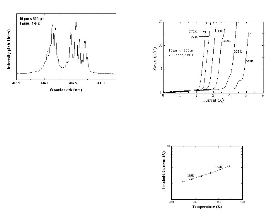
The sub-band emissions in the spectra shown in Fig-
ure 4 are known to be composed of many longitudinal
modes. [5] [10] Figure 6 is a spectrum obtained at a
higher resolution on the LD wit ha stripe of 10
µ
m x 800
µ
m. The sample was measured with a pulse width of 1
µ
sec at 1 kHz. It is observed that each sub-band consists
of several sharp peaks with a separation of 0.043 nm.
Assuming that these peaks arises from the longitudinal
modes of the LD, the mode separation
∆λ
is given by
∆λ
=
λ
o
2
/ 2Ln
where n is the effective refractive index,
λ
o
is the
emission wavelength, and L is the cavity length. Given
the values, 0.043 nm, 416.6 nm , and 800
µ
m for
∆λ
,
λ
o
,
and L, respectively, we obtained 2.52 as the refractive
index n. This value is close to a value calculated from
the optical modes of the structure and similar to a value
Nakamura et al. used in their early work on the pulsed
lasing. [11] However, somewhat larger effective refrac-
tive indexes of 3.3 and 3.6 have been reported in other
papers. [5] [10]
Figure 7a shows L-I characteristics of one of the
LD’s with a stripe of 10
µ
m x 1200
µ
m at different tem-
peratures ranging from 0 to 100
°
C. The pulse width
was 200 ns at 1 kHz. As shown in Figure 7a, the LD
lased up to a temperature as high as 100
°
C. However,
the LD showed a degradation phenomenon at 100
°
C. It
failed at greater current than 5 A. It is certain that with
increasing measurement temperature threshold current
increases. The temperature dependence of threshold
current is shown in Figure 7b. The calculated character-
istic temperature was 155K for around room tempera-
ture operation and 133K for higher temperature
operation. These values are comparable to those of other
group’s InGaN LDs. [5] [10] [12] Kuramata et al. has
reported a similar change in the characteristic tempera-
ture. [5] It is worth noting that the LD showed a kink in
the L-I plot at temperatures higher than 60
°
C with more
apparent appearance at higher temperature. Nakamura et
al. suggested that such a kink in the L-I plot for their
high power LD was due to the change in emission mode.
[13] More work is necessary to verify the origin of the
kink.
4 Conclusion
We demonstrated the room temperature pulsed lasing of
InGaN/GaN MQW blue LD grown by a multi-wafer
MOCVD system. Threshold current density was found
to be 20.3 kA cm
-2
for 10
µ
m x 800
µ
m stripe LD. The
operating voltage at this threshold current density was
16.5 V. Above the threshold current a strong and well-
defined emission mode with a peak spacing of 0.72 nm
was observed. The refractive index calculated from the
spacing between longitudinal modes was 2.52. The
measured characteristic temperature was between 130
and 150K.
REFERENCES
[1] S Nakamura, M Senoh, S Nagahama, N Iwasa, T
Yamada, T Matsushita, H Kiyoku, Y Sugimoto,
Jpn. J. Appl.
Phys.
35
, L74-L76 (1996).
[2] “InGaN/GaN/AlGaN-Based Violet Laser Diodes with a
Lifetime of More than 10,000 Hours”, S. Nakamura, M.
Senoh, S. Nagahama, N. Iwasa, T. Matsushita, and T. Mukai,
Proceedings of 2
nd
ISLLED, 371 (September 29 – October 2,
1998, Chiba, Japan)
[3] G.E. Bulman, K. Doverspike, S.T. Sheppard, T.W.
Weeks, H.S. Kong, H.M. Dieringer, J.A. Edmond, J.D.
Brown, J.T. Swindell, J.F. Schetzina,
Electron. Lett.
33
,
1556-1557 (1997).
[4] T. Kobayashi, F. Nakamura, K. Nagahama, T. Tojyo,
H. Nakajima, T. Asatsuma, H. Kawai, M. Ikeda,
Electron.
Lett.
34
, 1494 (1998).
[5] A. Kuramata, S. I. Kubota, R. Soejima, K. Domen, K.
Horino, T. Tanahashi,
Jpn. J. Appl. Phys.
37
, L1373 (1998).
[6] I. Akasaki, S. Sota, H. Sakai, T. Tanaka, M. Koike, H.
Amano,
Electron. Lett.
32
, 1105-1106 (1996).
[7] K. Itaya, M. Onomura, J. Nishio, L. Sugiura, S. Saito,
M. Suzuki, J. Rennie, S. Nunoue, M. Yamamato, H.
Fujimoto, Y. Kokobun, Y. Ohba, G. Hatakoshi, M. Ishikawa,
Jpn. J. Appl. Phys.
35
, l1315-l1317 (1996).
[8] M.P. Mack, A. Abare, M. Aizcorbe, Peter Kozodoy , S.
Keller, U. K. Mishra, L. Coldren, Steven DenBaars ,
MRS
Internet J. Nitride Semicond. Res.
2
, 41 (1997).
[9] Y. Kimura, M. Miyachi, K. Takahashi, T. Tanaka, M.
Nishitsuka, A. Watanabe, H. Ota, K Chikuma,
Jpn. J. Appl.
Phys.
37
, L1231 (1998).
[10] S Nakamura, M Senoh, S Nagahama, N Iwasa, T
Yamada, T Matsushita, Y Sugimoto, H Kiyoku,
Appl. Phys.
Lett.
70
, 1417-1419 (1997).
[11] Shuji Nakamura, Gerhard Fasol,
The Blue Laser Diode
- GaN based Light Emitters and Lasers
, (Springer-Verlag,
Heidelberg, 1997), .
[12] S. Nakamura, M. Senoh, S. Nagahama, N. Iwasa, T.
Yamada, T. Matsushita, Y. Sugimoto, H. Kiyoku,
Appl. Phys.
Lett.
69
, 3034-3036 (1996).
[13] S. Nakamura, M. Senoh, S. Nagahama, N. Iwasa, T.
Yamada, T. Matsushita, H. Kiyoku, Y. Sugimoto, T. Kozaki,
H. Umemoto, M. Sano, K. Chocho,
Jpn. J. Appl. Phys.
37
,
L627 (1998).
MRS Internet J. Nitride Semicond. Res. 4, 1 (1999). 3
© 1999 The Materials Research Society
FIGURES
Figure 1. A schematic of the fabricated LD
Figure 2. L-I-V characteristic of the LD
Figure 3. Polarized light output intensity of the LD.
Figure 4. Spectra of the pulsed lasing
Figure 5. A far-field pattern of pulsed lasing.
4 MRS Internet J. Nitride Semicond. Res. 4, 1 (1999).
© 1999 The Materials Research Society
Figure 6. Subband emission consisting of sharp longitudinal
modes.
Figure 7a. Temperature dependence of L-I characteristics of the
LD
Figure 7b. Threshold current as a function of measurement
temperature.
