197
Fabrication and Characterization of Two Compliant Electrical Contacts for MEMS:
Gallium Microdroplets and Carbon Nanotube Turfs
Y. Kim, A. Qiu, J. A. Reid, R.D. Johnson, and D. F. Bahr
Mechanical and Materials Engineering, Washington State University, Pullman WA USA
ABSTRACT
Because of their high mechanical compliance and electrical properties, the idea of using
Ga and CNTs for micro electrical relay contacts has been investigated to minimize damage from
switching and make good electrical contacts. Ga was electroplated into droplets on the order of
50 Pm in radius on single crystal Si to create a contact for a switch that can be annealed to
recover its original electrical properties after mechanical damage. CNTs were grown on Si
substrates, coated with a thin Au layer, and transferred to other Si or Kapton substrates through
thermocompression bonding. In the case of the Ga contact, repeated switching led to an increase
in the resistance, but the resistance recovered after a thermal reflow process at 120 °C. Longer
term and larger area contacts were used to measure the contact behavior under switching
conditions of up to 200 A/cm
2
. At moderate cycling conditions (on the order of 200 cycles) the
adhesion began to significantly degrade the switch. The oxidation behavior of the Ga droplets
was characterized for thermal reflow, suggesting a passivating 30 nm oxide forms at 100 °C. The
oxide formed by the Ga is thin and fragile as demonstrated by its use in a switch. The Ga
droplets were examined with electrical contact resistance nanoindentation and the loads at
fracture and the onset of electrical contact were identified. CNT turfs were also tested for making
patterned electrical contacts; turfs of lateral dimensions similar to the Ga droplets were tested
using electrical resistance testing during nanoindentation and as macroscopic contacts, and
shown to be able to carry similar current densities. The results will be compared between the two
systems, and benefits and challenges of each will be highlighted for creating compliant electrical
switches and contacts.
INTRODUCTION
Micro electro mechanical systems (MEMS) cover a broad base of systems which use
processing developed for microelectronics processing to fabricate devices with both electrical
and mechanical functionality [ 1 ]. There are various types of micromechanical switches in
MEMS [2, 3, 4]. These switches are useful in applications for a wide operating temperature
ranges, radiation insensitivity, and usually have a high on-off impedance ratio. Ideally when the
switch is closed it will exhibit good electrical and thermal. Almost all micromechanical switches
have been designed with solid-to-solid contacts [5], and traditionally suffer from problems such
as contact bounce, noise, high contact resistance, slow rise times, and a short operational lifetime
due to mechanical wear and tear [ 6 ]. These problems may be solved by using compliant
materials because they can exhibit a fast signal rise time, form high contact area at low applied
loads, high thermal conductivity, and in some cases a low contact resistance [6, 7, 8]. Gallium
(Ga) and carbon nanotube arrays (CNTs) are representative compliant materials. Gallium (Ga)
proves to be a promising liquid metal above 29 ˚C, as its high boiling point (approximately 2400
˚C) allows for Ga to be used in high current and high temperature applications. Small confined
droplets of Ga have been studied on the nanoscale and have mechanical responses that imply a
DOI: 10.1557/opl.2011.533
Mater. Res. Soc. Symp. Proc. Vol. 1299 © 2011 Materials Research Society

198
non-zero shear modulus even when liquid [9]. CNT turfs have been used for a wide variety of
applications as an electrically conducting medium [10]. CNT turfs, arrays of CNTs in nominally
vertical orientations, have been shown to be more compliant than carbon nanofiber arrays [11].
Therefore, this current study will focus on Ga and CNT turfs as compliant materials for electrical
contacts in MEMS.
EXPERIMENT
Figure 1 shows the schematic process flow and fabrication of the Ga samples. The
samples were fabricated from single side polished 3 inch diameter (100) boron doped silicon (Si)
wafers. Silicon dioxide (SiO
2
) was grown as a thin (120-180 nm) oxide layer using wet oxidation
after boron doping. After patterning with photoresist, the oxidation layer of the sample was
etched in Buffered Oxide Etch (BOE). A 10nm thick titanium / tungsten (Ti/W) adhesion layer
was DC sputtered on the wafer, and 100nm thick W was then sputtered on the wafer. After
photolithography the metal layers were etched in H
2
O
2
. Finally, the wafer was cleaned with with
acetone, isopropyl alcohol, and deionized (DI) water and diced.
(A)
(B)
(C)
PR
(D)
(E)
W
(F)
(G)
(H)
Figure 1. The process flow and the fabricated structure for Ga. (A) Boron doping, (B) Oxidation,
(C) Patterning the oxide surface with the photoresist (PR), (D) Etching the patterned oxide layer
in BOE, (E) sputtering Ti/W and W, (F) Patterning the W surface with PR, (G) Etching the W
layer in H
2
O
2
, (H) Electroplating Ga on the sample.
The electrolyte consisted of gallium chloride and 140 ml solution of deionized (DI) water
and hydrochloric acid (HCl). The pH of the solution was kept between 1.5 and 2.5, adjusted by
adding HCl, and the concentration of gallium was 2.5M. The conditions for the most uniform
deposition used a current density, a cathode current, and a cathode potential of 1A/cm
2
, between
0.06A and 0.09A, and -0.6 to -0.7 V respectively, and the temperature was kept between 40˚-
50˚C. A platinum wire and the sample were placed in a glass beaker as a H
2
evolution anode and
cathode respectively [12]. Ga selectively plated on the W surfaces with only small amounts
depositing on the B doped Si.
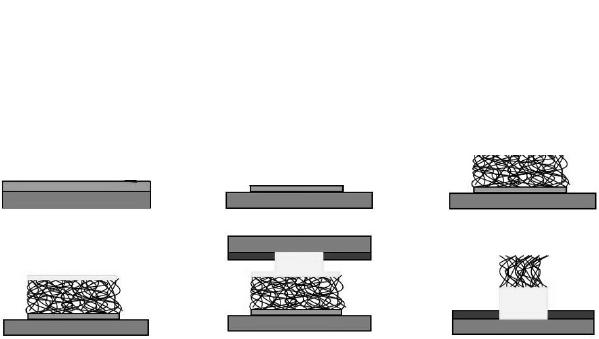
Figure 2 schematically shows the process flow and the fabricated structures for CNT turfs
samples. Patterned CNT turfs were prepared with photolithography to create turfs 200 μm
diameter with a height of approximately 20 μm. A sol gel of TEOS with solute Fe was deposited
on clean silicon wafers in a manner described previously [13]. The individual tubes on these turfs
are on the order of 15 nm in diameter and are multi-walled with 3-6 walls, previously identified
using transmission electron microscopy. The turfs were grown in a tube furnace using chemical
B Dope

199
vapor deposition at a pressure of 100 mbar and temperature of 973 K, with a gas flow of
385sccm hydrogen and 25sccm ethylene. Growth time was varied between 30 and 60 minutes,
and the heights of the turfs were between 21 and 23 μm. The tops of the CNT turfs were coated
with a 5 nm Ti/W adhesion layer and 300 nm Au film, and then the CNT turfs were transferred a
Si wafer coated with a 5 nm Ti/W and 300 nm Au film through thermocompression bonding at
150 ˚C for 2 hours [14].
(A)
Sol-gel
(B)
(C) CNT turfs
(D)
Ti/W and Au layer
(E)
(F)
Figure 2. The process flow and the fabricated structure for CNT turfs. (A) Depositing sol gel on
Si wafer, (B) Patterned sol gel, (C) Growth of the CNT turfs, (D) Sputtering Ti/W and Au on the
tops of the CNT turfs, (E) Thermocompression bonding with patterned Au film, (F) Transferred
CNT turfs to the patterned Au film. Procedures described in [14].
The thermal reflow of Ga was carried out in a furnace and ambient atmosphere. Reflow
test samples were put in a pre-heated furnace. After the desired time was reached, the samples
were cooled by switching off the furnace. To analyze the oxidation of the Ga structures that may
occur during operation, TGA was carried out using a Rheometrics STA 650. Samples were
placed in open crucibles in oxygen gas and were heated at 10 ºC/minute to determine if the oxide
was passivating.
To apply a voltage to the test sample, a W probe was affixed to the bonding pad, and the
Ga droplets were contacted with other W probe (for short term) and with an aluminum sphere tip
(for long term) in a compression test fixture to measure both load and displacement during
contact. The current values were measured with a digital oscilloscope by monitoring the voltage
across a resistor in parallel. A load of 0.5 N was applied for long term switch. Electrical contact
resistance (ECR) nanoindentation in a Hysitron Triboidenter was used with a boron doped
diamond tip to monitor the resistance during the initial stages of contact between a probe and the
Ga droplets or CNT turfs. In this case the voltage and current were monitored using a Keithley®
model 2602 dual channel system SourceMeter. The ECR nanoindentater was used for the effect
of the current density as a function of force.
A voltage of 2V was applied for ECR testing.
RESULTS and DISCUSSION
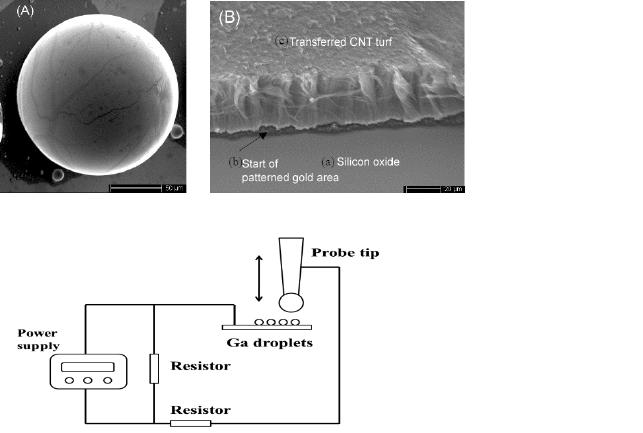
Figure 3 shows scanning electron microscope (SEM) images of electroplated and
annealed Ga droplet, and the patterned and transferred CNT turfs. In general, before thermal
reflow the surface of the deposited Ga droplet was rough, but after thermal reflow the surface
was relatively smooth, and the droplet became relatively spherical in shape (Figure 3A).

200
Figure 4. Schematic of the bulk
electrical test set up.
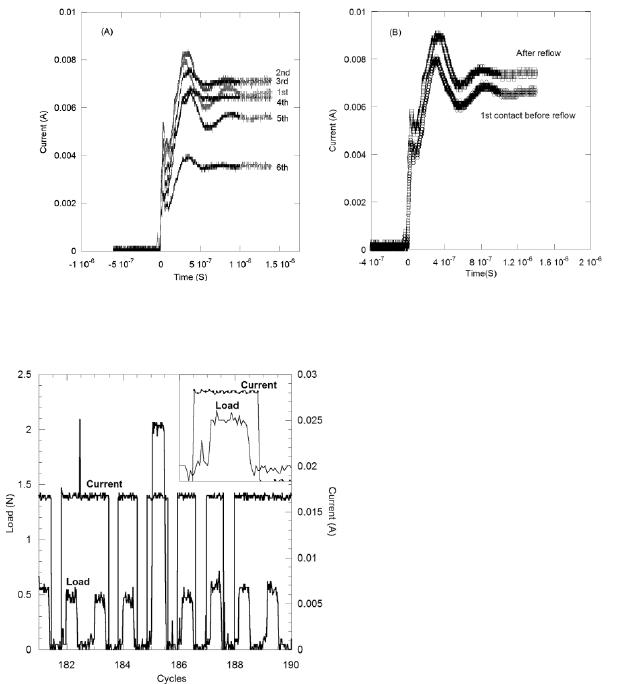
The schematic of the test set up is shown in figure 4. Figure 5 shows the typical electrical
performance of the Ga droplet switch at a constant voltage (3V DC) as a function of time with a
W tip. Repeated switching on multiple droplets showed that the second contact always exhibited
a lower resistance contact due to flattened the contact surface (leading to a larger contact area)
after the first contact. However, the steady state resistance increases with the third and further
contacts, as shown in figure 5 (A). It is assumed that this is because of plastic deformation and
sub-surface defect generation. Subsequent thermal reflow (figure 5 (B)) “heals” the switch back
to the initial performance level, suggesting damage to the switch is removed during reflow,
previously identified using SEM [15].
Longer term and larger area contacts were used to measure the contact behavior under
more realistic switching conditions. The contact was cycled at 0.4 Hz in depth control to apply a
nominal load of 0.5 N (large enough to cause plastic deformation), and the applied load and
current through the switch were monitored. This magnitude of contact leads to approximately
four Ga droplets coming into contact with the aluminum probe tip, a total contact area of
approximately 50 Pm in radius, and a load of approximately 125 mN per droplet. The resulting
current density of the switch for this test was approximately 200 A/cm
2
. Each cycle produced an
open and closed cycle until cycle 182. At cycle 182 the switch remained closed while the load
was removed, suggesting material had transferred to the aluminum contact and fibers of Ga were
bridging the gap.
Figure 3. SEM
pictures of (A)
electroplated gallium
(Ga) droplets after
thermal reflow at
100ȋC for 10 min
and (B) patterned
and transferred CNT
turfs.

201
Figure 5. The short term switching behaviors of the Ga droplet: (A) First series of electrical
switching tests showing degradation with continued switching. (B) Electrical performance
after thermal reflow at 120 ȋC, where performance now exceeds the initial conditions.
Figure 6 shows the load and current during switching at cycle 182. The maximum load
increased at cycle 185 in figure 6. The inset in figure 6 shows the switch turns on when the load
begins to increase and remains on while the load decreases. In case of the solid-to-solid contacts,
this phenomenon is exhibited when the contact surface has a clean and flat surface. According to
Dickrell et al., a conductive contamination layer can develop with repeated contact during long
term switching [16]. They implied that the contamination layer can be breached by added force.
To examine the oxide thickness, after the switch was annealed at elevated temperatures
TGA was performed. TGA analysis of a Ga sample was completed in oxygen. The sample was
heated to 115 qC over the course of one hour (similar to the annealing conditions to recover the
performance of the switch). TGA weight gain curves show gallium forms a protective oxide at
Figure 6. Cyclic
mechanical switching at
0.5 V using Ga switch
in contact with
aluminum sphere at
nomimal contact load of
0.5 N, inset shows cycle
186.

202
temperatures above ambient. Using the number of droplets and weight gain, the oxide thickness
after annealing in oxygen is estimated to be 30 nm. A thin oxide supported on a compliant
substrate suggests that pressures in excess of those needed to cause permanent deformation of the
substrate would cause fracture any passivation layer and make electrical contact in this system.
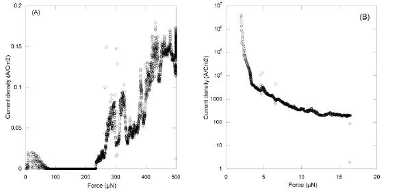
Figure 7. The current density values as function of force for (A) Ga and (B) CNT turfs using
the ECR nanoindentation test.
Figure 7 shows the current density of a Ga droplet and CNT turfs as a function of force
by ECR nanoindentation testing. The area of indentation was assumed to be equivalent to the
area function of the diamond tip (i.e. to first order this ignores pile up and sink in) The current
density value of Ga at a maximum force of 500 μN (3000 nm depth) was approximately 0.175
A/cm
2
, whereas that of CNT turfs at 16 μN (200 nm depth) was approximately 190 A/cm
2
. For
the Ga droplet, as the force increased, the current density also increased except for the force
range of 70 to 220 μN in figure 7 (A). The drop in current density in Figure 7(A) may be due
to contamination of the oxide layer on the surface of the Ga droplet, and the subsequent rise in
current would likely be attributed to the oxide film breaking. On the other hand, in the case of
the CNT turfs, Figure 7(B), the current density decreased with an increase in the force because
the resistance was increasing with increased contact area. We suspect this is due to significant
adhesion at the beginning of the indentation with an underestimate of the actual contact area at
the start of the indent; this will be the subject of a future study. The current density carried by
the CNT turfs was significantly higher than that of the Ga droplet.
CONCLUSIONS
The suitability of a Ga micro-droplets and CNT turfs for compliant electrical contacts in
MEMS was investigated by characterizing the electrical performance and nanoindentation
behavior of the structures. Smooth Ga droplets can be formed using electroplating and thermal
reflow processing at moderate temperatures. The electrical resistance of the Ga droplets
increased due to mechanical deformation, but returned to the initial value after thermal reflow.
The oxide on the Ga droplet formed by this thermal reflow is easily fractured with applied
203
pressure to make electrical contact. Larger contacts could be run for over 100 cycles with no
significant increase in resistance. In the larger contacts, the current density of Ga was
approximately 200 A/cm
2
. The current density measured using ECR nanoindentation increased
as the applied force increased, whereas that of CNT turfs decreases as the force increased.
However, the values of CNT turfs were significantly higher than that of Ga. Therefore,
electroplated Ga micro droplets and CNT turfs may be used for electrical switches and contacts
because moderate damage that may occur during switching of Ga droplets can be eliminated with
a moderate thermal reflow process, and the CNT turfs can carry high current density under a
very small amount of applied force.
ACKNOWLEDGEMENTS
This work was supported in part (AQ and DFB) by the National Science Foundation
under the NIRT program, grant CMMI-0856436.
REFERENCES
1. A. Witvrouw, H.A.C. Tilmans, and I. De Wolf, Microelectron. Eng. 76, 245 (2004).
2. K. Petersen, Proc. of the IEEE 70, 420 (1982).
3. S. Roy, and M. Mehregany, IEEE MEMS Workshop, 353 (January-February 1995).
4.
E. Hashimoto, Y. Uenishi, and A. Watabe, Proc. Int. Solid-State Sensor Actuator, 361 (June
1995).
5.
J. Kim, W. Shen, L. Latorre, and C.J. Kim, Sensor Actuator A 97-98, 672 (2002).
6. J. Simon, S. Saffer, and C.J. Kim, IEEE MEMS'96 Proc., 515 (1996).
7. M.M.J. Treacy, T.W. Ebbesen, and J.M. Gibson, Nature 381, 678-680 (1996).
8 . P. Kim, L. Shi, A. Majumdar, and P.L. McEuen, Phys. Rev. Lett. 87, 215502 (2001).
9.
J. B. Huang, G. T. Fei, J. P. Shui, P. Cui, and Y. Z. Wang, Phys. Status. Solidi. A 194, 167
(2002).
10. F. Kreupl, A.P. Graham, G.S. Duesberg, W. Steinhögl, M. Liebau, E. Unger, and W. Hönlein,
Microelecron. Eng. 64, 349-408 (2002).
11. M. Terrones, N. Grobert, J. Olivares, J.P. Zhang, H. Terrones, K. Kordatos, W.K. Hsu, J.P.
Hare, P.D. Townsend, K. Prassides, A K. Cheetham, H.W. Kroto, and D.R.M. Walton,
Nature 388, 52-55 (1997).
12. S. Sundararajan and T.R. Bhat, J. Less-common Met., 11, 360-364 (1966).
13. C.M. McCarter, R.F. Richards, S. Mesarovic, C.D. Richards, D.F. Bahr, D. McClain, J. Jiao,
J. Mater. Sci., 41, 7872-7878 (2006).
14. R.D. Johnson, D.F. Bahr, C.D. Richards, R.F. Richards, D. McClain, J. Green, and J. Jiao,
Nanotechnology, 20, 065703, 6 (2009).
15. Y. Kim and D.F. Bahr, Mater. Res. Soc. Proc. 1139, (Boston, MA, 2008) GG03-05.
16 . D.J. Dickrell, and M.T. Dugger, IEEE Trans. Compon. Packag. Technol. 30, 75 (2007).
