Mater. Res. Soc. Symp. Proc. Vol. 1750 © 2015 Materials Research Society
DOI: 10.1557/opl.2015.
A simulation study for defects in sub-15 nm line-space using directed self-assembly
Hideki Kanai, Katsuyoshi Kodera, Yuriko Seino, Hironobu Sato, Yusuke Kasahara,
Katsutoshi Kobayashi, Ken Miyagi, Shinya Minegishi, Naoko Kihara, Yoshiaki Kawamonzen,
Tomoharu Fujiwara, Noriyuki Hirayanagi, Toshikatsu Tobana and Tsukasa Azuma
EUVL Infrastructure Development Center, Inc. (EIDEC),
16-1 Onogawa, Tsukuba, Ibaraki, 305-8569, Japan
ABSTRACT
A specific type of buried defect in lamellar phase diblock copolymer was studied by
experiments and simulations using self-consistent field theory (SCFT). The defects had 3-
dimensional structures and created hexagonally arranged holes. They existed not only on the
substrate with the guide structures but in fingerprints. The simulation results suggested that one
of the causes of the defects is mismatch of the surface affinity of the neutral layer.
INTRODUCTION
Recently, directed self-assembly (DSA) with lamellar phase block copolymer has
progressed greatly with regard to its applicability in the manufacturing of semiconductor devices,
but the topological defects such as dislocation and disclination remain a major concern. In
addition, buried defects [1-3] may appear if the materials and/or the process steps are not
optimized for chemo- or grapho-epitaxy flow, and then they will cause poor etch selectivity and
degradation of line edge roughness (LER) in pattern transfers into underlayers. Hexagonally
perforated lamellae (HPL), one of the typical types of the buried defects, has been investigated
with experiments [4] and simulations [5, 6]. HPL is recognized as a metastable state and can be
seen with diblock and triblock copolymers.
In this study, we discuss defect analysis, in which specific type of buried defect is
included. The buried defects arise and are clearly evident on shallowly etched SOG after dry
development of PS-b-PMMA diblock copolymers. The analysis is based on self-consistent field
theory (SCFT) simulation for the bottom surface affinity with analysis of free energy difference
among several phase configurations.
EXPERIMENTAL DETAILS
PS-b-PMMA diblock copolymers with 1/2∙L
0
= 15 nm (L
0
is pitch of the copolymers)
and OH-terminated PS-r-PMMA as the neutral layer were used. The substrate consisted of spin-
on-glass (SOG) and spin-on-carbon (SOC) stacked on bare-Si. The EIDEC process flow
described in ref. 7 for making 15 nm half-pitch lines and spaces on 90 nm pitch guide structures
is as follows. Firstly, photoresist is coated on SOG/SOC stacked wafer and exposed by a novel
ArF immersion scanner. The photoresist and the SOG are etched in order to reduce the width to
1/2∙L
0
. The trimmed photoresist and the SOG work as chemical guides and affinity to PMMA
segment of the PS-b-PMMA is induced. They also work as physical guides of grapho-epitaxy.
Then, the neutral layer is spin-coated and grafted only on the SOG surface and PS-b-PMMA is
coated and thermally annealed to induce microphase separation. Finally, the PMMA is removed
by RIE and 15 nm PS lines are formed. In this flow, no special pinning material or photoresist
361
stripping process is needed because the SOG and photoresist are utilized for pinning and the
photoresist is removed naturally through the RIE process. However, the affinity of the resist
surface must be controlled to play the role of pinning and align fine 15 nm lines and spaces
without defects.
Grid defects
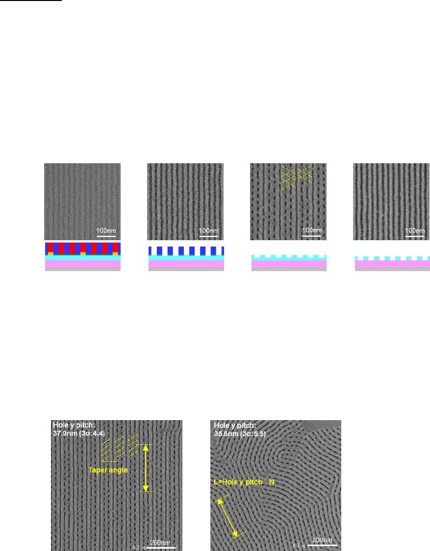
Figure 1 shows CD-SEM images at each process step after microphase separation. Line-
and-space structures before and just after dry development of the diblock copolymers (Fig.1 (a),
(b)) look finely aligned and it is hard to find any PS shorts or bridges. However, grid defects are
clearly observed on the shallowly etched SOG as shown in Fig. 1 (c). With regard to their
configuration, the defects are almost perfectly hexagonally arranged holes with slightly
elongated pitch in Y-direction (vertical direction in the image). They look as if they were
intentionally fabricated, but in fact were not. The defects almost disappeared after SOG full etch
(Fig. 1 (d)), but they are potential problem that should be fixed. The results of this experiments
indicate that the PS bridges are hidden but exist after microphase separation and they are realized
by the SOG etch. The defects are ameliorated by longer annealing time with higher temperature
as described in ref. 7.
(a) (b) (c) (d)
Figure 1. Topdown CD-SEM images at each process step: (a) after microphase separation, (b) after
dry development (PMMA removal), (c) after SOG shallow etching, (d) after SOG full etching,
structures in colors represent PMMA (red), PS (blue), pinning resist (orange), neutral layer (green),
SOG (light blue), SOC (magenta).
In fact, the grid defects are also found in the case of fingerprint without any guides post
SOG shallow etch (Fig. 2). Since the grid defects are periodic structures that exist in fingerprints,
profile of the guide structure or mismatch in dimensions between guide pitch and L
0
are not the
main cause. They are thought to originate from surface conditions of the neutral layer or an issue
concerning the diblock copolymer itself.
(a) (b)
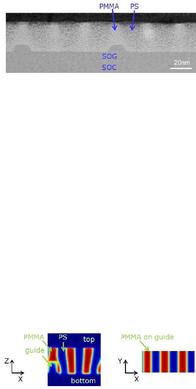
Figure 2. Images of grid defects with and without guides: (a) with guide structure, holes are
almost hexagonally arranged but slightly elongated in Y-direction (vertical), (b) grid defects are
found in fingerprints without guide structures.
Figure 3 shows a cross-sectional TEM image with good image contrast between PS and
PMMA. This is a thin film image but looks as if it were not thin enough with high acceleration
voltage. The PS bridges are still unclear and we can only speculate on the configurations of the
PS and the PMMA domains.
Figure 3. A TEM image using 300 kV acceleration voltage and contrast enhancement by dyeing.
The brighter portions are PMMA and the darker portions are PS.
SIMULATION METHOD
3-dimensional SCFT simulations were executed. Symmetric AB block copolymer is
modeled as a standard continuous Gaussian chain composed of segments A and B, where the
numbers of the A segment N
A
= 10 and the B segment N
B
= 10. The interaction between A and B
is mediated through the Flory-Huggins parameter χ. In this work, we adopted χN = 20, where χ
= 1 and the total number N = 20. In the case of PS-b-PMMA, a reference value of χN = 20
roughly corresponds to forming lamellar pitch 1/2∙L
0
= 15 nm for the annealing temperature of
250
o
C.
Figure 4 shows a structure obtained by the simulation. The AB diblock copolymers were
confined by 3 walls represented by top, bottom and pinning layers. Each wall portion was filled
with homopolymers, where each number N
w
was 1 in this simulation. Periodic boundary
conditions were imposed in all directions. The pitch of the guide in X-direction was 3∙L
0
and the
copolymer film thickness corresponding to the distance between the bottom and the top layers in
Z-direction was 3/2∙L
0
. The guide height was 0.68∙L
0
and width was 0.48∙L
0
.
Figure 4. An example of an image of the simulation. In this case, the morphology is lamellar.
X-Z plane is on the left and X-Y plane is on the right.
The interactions between each diblock copolymer segment and each wall (top, bottom,
pinning) were modeled by Flory-Huggins-like interactions as well. We defined 6 affinity
parameters χ
btm-A
, χ
btm-B
, χ
top-A
, χ
top-B
, χ
pin-A
, χ
pin-B
called surface chi parameters. χ
btm-A
represents
interactions between the bottom wall and the A segment, and the other parameters represent the
interactions in the same way. If χ
btm-A
is smaller than χ
btm-B
, the bottom surface has preferential
affinity to A segment. On the other hand, if χ
btm-A
is bigger than χ
btm-B
, it has preferential affinity
to B segment. Therefore, we could model surface wetting conditions of the walls. The
parameters χ
btm-A
, χ
btm-B
, χ
top-A
, χ
top-B
, χ
pin-A
, χ
pin-B
were 2, 2, 2, 2, 1, 2, respectively unless
otherwise noted. Please note that A was PMMA and B was PS. The pinning is assumed to have
affinity to PMMA because PMMA domain is above the pinning.
Although researchers usually run SCFT simulations with random initial mean field
conditions in order to obtain the most stable equilibrium state having the minimum free energy,
the free energy usually has some local metastable states and the calculation is trapped in one of
the metastable states. Different initial mean fields often result in different metastable states. By
carefully giving initial conditions, some typical metastable states could be obtained. In this study,
we evaluated not only the most stable diblock structures but also the energy gap ΔE between the
most stable state and metastable states, which enabled us to evaluate appearance of the states
after the microphase separations [8].
The initial values of the self-consistent mean fields V
k,initial
(x,y,z) are given by
V
k,initial
(x,y,z) = θ
K
(x,y,z) + f
K
(x,y,z) where k denotes the species type (k = 0,1,2,⋯,N-1), θ
K
(x,y,z) is a Gaussian random noise function and f
K
(x,y,z) is a function to adjust the initial
distribution of the self-consistent field. For example, when f
K
(x,y,z) is a periodic function with
period Λ along x-axis (f
K
(x+Λ,y,z) = f
K
(x,y,z)), the phase configuration can easily converge
toward lamellar structure along x-axis as well. It should be noted that f
K
(x,y,z) and the number of
iterations should be decided carefully in order to obtain consistent results.
SIMULATION RESULTS
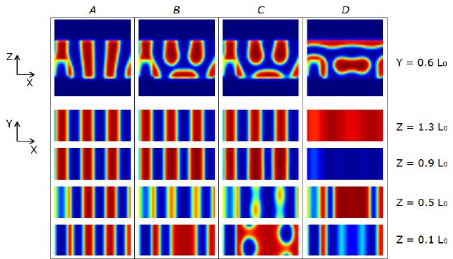
Three conditions of the bottom surface were evaluated (Fig. 5-7). Figure 5 shows the case
of neutral bottom surface, where the surface chi parameters were the default values as mentioned
above. The image of X-Z plane is the image sliced at the center of Y, and the four X-Y plane
images are images sliced at different Z positions, where Z = 0 is the boundary of the bottom and
the copolymers. Magnitude of free energy for each configuration is A << B < C << D and the
regular lamellar phase (5A) has the minimum free energy and can be seen on wafers.
Figure 5. In the case of neutral bottom surface, some configurations A to D originate from some
initial conditions. Magnitude of each free energy is A << B < C << D and A has the minimum
free energy and can be seen.
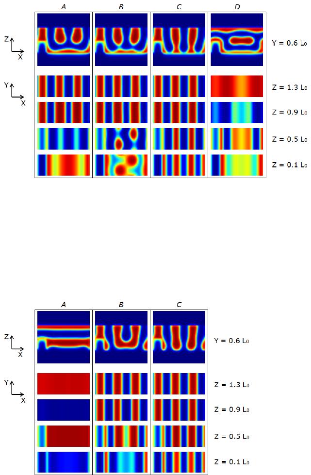
Figure 6 shows the case of the bottom surface has affinity to PMMA, in which χ
btm-A
is
changed from 2 to 1, the free energy indicates that A has the minimum and B is comparable to A.
C is closer to regular lamellae (e.g. Fig. 5A) but the free energy analysis suggests it is difficult
for C to exist. A has horizontal PMMA and PS domains over the bottom surface and straight
lines-and-spaces seen from the top. B shows the PMMA domain arrangement is hexagonal holes
and looks like the grid defects. In Fig. 5-7, the Y-pitch is ~1.2∙L
0
and the periodic boundary
condition is used. Therefore the hole Y-pitch is assumed to be half of 1.2∙L
0
in Fig. 6B.
Figure 6. In the case of bottom surface affinity to PMMA, some configurations A to D originate
from some initial conditions. Magnitude of each free energy is A ~ B < C << D and A and B have
a chance to exist.
If the bottom surface has affinity to PS (Fig. 7), in which χ
btm-B
is changed from 2 to 1,
the PS domain is laid on the bottom surface and horizontally aligned lamellae are observed. Of
course, they must be related to magnitude of the affinity and might be too strong. However, the
affinity to PS may not cause the defect.
Figure 7. In the case of bottom surface affinity to PS, some configurations A to C originate from
some initial conditions. Magnitude of each free energy is A << B < C.
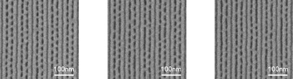
In order to evaluate the effect of affinity of the neutral layer on the grid defects, three
neutral layers were prepared. Their contact angles of water were 80.5
o
, 81.9
o
and 84.4
o
,
respectively. The layer with C.A. 80.5
o
was identical to it used in the foregoing experiments.
Figure 8 shows SEM images of the grid defects on each neutral layer. The PS bridges between
PS lines decreased according to the C.A. and the neutral layer having the most affinity to PS (Fig.
8 (c)) showed clearly improved appearance of the defects. This suggests that greater affinity to
PS is preferable to reduce the grid defects, which is coincident with the simulation results.
(a) (b) (c)
Figure 8. Three degree of affinity of neutral layer surface: (a) water C.A. = 80.5
o
(b) water C.A.
= 81.9
o
(c) water C.A. = 84.4
o
CONCLUSIONS
The SCFT simulations were executed to analyze the causes of the grid defects. One of the
possible causes is mismatch of surface affinity of the neutral layer. If the surface has affinity to
PMMA, the free energy difference of the lamellae and the defects would decrease and the defects
would tend to be observed. This suggestion was confirmed by experimental results showing that
the neutral layer with greater affinity to PS was improved.
ACKNOWLEDGMENTS
We used OCTA (http://octa.jp) software in order to acquire some of our simulation
results. A part of this work was funded by the New Energy and Industrial Technology
Development Organization (NEDO) under the EIDEC project. We would like to thank Mr.
Satoshi Nomura for technical supports.
REFERENCES
1. Marcus Müller, Kostas Ch. Daoulasa, Yuki Norizoe, Phys. Chem. Chem. Phys., 11, 2087 (2009).
2. Chi-Chun Liu, Abelardo Ramírez-Hernández, Eungnak Han, Gordon S. W. Craig, Yasuhiko Tada,
Hiroshi Yoshida, Huiman Kang, Shengxiang Ji, Padma Gopalan, Juan J. de Pablo, Paul F. Nealey,
Macromolecules, 46 (4), 1415 (2013).
3. Richard A. Farrell, Erik R. Hosler, Gerard M. Schmid, Ji Xu, Moshe E. Preil, Vinayak Rastogi,
Nihar Mohanty, Kaushik Kumar, Michael J. Cicoria, David R. Hetzer, Anton DeVilliers, Proc. SPIE,
9051, 90510Z (2014).
4. Moon Jeong Park, Nitash P. Balsara, Macromolecules, 41, 3678 (2008).
5. M. W. Matsen, R. B. Thompson, J. Chem. Phys., 111 (15), 7139 (1999).
6. Pavel Petrus, Martin Lísal, John K. Brennan, Langmuir, 26 (18), 14680 (2010).
7. Yuriko Seino et. al., The 40th International Conference on Micro and Nano Engineering (MNE
2014), 8076 (2014); 27th International Microprocesses and Nanotechnology Conference (MNC
2014), 7A-9-1 (2014).
8. Katsuyoshi Kodera et.al., Journal of Photopolymer Science and Technology, 27 (1), 31 (2014);
Proc. SPIE 9049 904926 (2014).
