
http://journals.cambridge.org Downloaded: 11 Mar 2015 IP address: 203.64.11.45
Microstructure and misfit relaxation in SrTiO
3
/SrRuO
3
bilayer films on LaAlO
3
(100) substrates
J.S. Wu,
a)
C.L. Jia, and K. Urban
Institut fu¨r Festko¨rperforschung, Forschungszentrum Ju¨lich GmbH, D-52425 Ju¨lich, Germany
J.H. Hao and X.X. Xi
Department of Physics, The Pennsylvania State University, University Park, Pennsylvania 16802
(Received 12 March 2001; accepted 12 September 2001)
We studied the microstructure of SrTiO
3
/SrRuO
3
bilayer films on (001) LaAlO
3
substrates by high-resolution transmission electron microscopy. At the SrRuO
3
/LaAlO
3
interface a defect configuration of stacking faults and nanotwins bounding either Frank
partial dislocations or Shockley partial dislocations and complex interaction between
these planar defects were found to be the dominant means of misfit accommodation.
The misfit in the SrTiO
3
/SrRuO
3
system, however, is mainly accommodated by
elastic strain. Most of the observed defects in the SrTiO
3
layer can be related to the
{111} planar defects in the SrRuO
3
layer propagating and reaching the SrTiO
3
/SrRuO
3
interface. Furthermore, a {110} planar defect can also be introduced in the SrTiO
3
layer due to the structure change of the SrTiO
3
/SrRuO
3
interface.
I. INTRODUCTION
The deposition of high-quality perovskite ceramic thin
films for various applications is one of the most active
areas in materials research. SrRuO
3
has attracted consid-
erable interest in recent years due to its good conductiv-
ity, high chemical and thermal stability, and excellent
lattice match with many other electroceramic materials
such as SrTiO
3
and YBa
2
Cu
3
O
7
.
1–6
In superconducting
devices, SrRuO
3
films have been used as buffer layers
for the growth of high-temperature superconducting
YBa
2
Cu
3
O
7−x
films and also as a barrier layer in Joseph-
son junctions.
3,4
In ferroelectric nonvolatile memory ap-
plications, they have been employed as electrodes.
5,6
The
microstructure and defects in the SrRuO
3
layer are im-
portant since they can have a considerable effect on the
device layers which directly connect to the SrRuO
3
layer.
It is known that SrTiO
3
is an interesting dielectric
material and suitable for various applications such as
voltage tunable filters, oscillators, and phase shifters for
microwave circuits.
8,9
However, the properties of SrTiO
3
thin films which are necessary for device applications are
not as good as those of bulk single crystals. Their tun-
ability is lower and the dielectric losses are high.
10,11
Recently, with employment of SrRuO
3
as the buffer
layer, high-quality SrTiO
3
films with near single-crystal
level dielectric loss were successfully prepared on
LaAlO
3
substrates.
12
Besides perfect dislocations, partial
dislocations including both Shockley-type with Burgers
vectors inclined to the interfaces and Frank-type in the
interfaces were proposed as effective means of misfit
relaxation in the heterostructure system.
13
The dissocia-
tion of 60° dislocations in epitaxial semiconductor films
and the role of the resulting partials in misfit relaxation
have been well established. Partial dislocations of
a/2〈101〉 type accompanied by stacking faults in the
(010) plane have been observed in several perovskite
films.
14–17
At room temperature SrRuO
3
is a distorted perovskite
with orthorhombic lattice and has a pseudocubic lattice
parameter of 0.3928 nm. SrTiO
3
has perovskite cubic
structure with a ⳱ 0.3905 nm. The substrate, LaAlO
3
,is
a rhombohedrally distorted perovskite, and its pseudocubic
parameter is 0.3790 nm. On the basis of the lattice para-
meter values the lattice mismatch between SrRuO
3
and
LaAlO
3
is 3.6%, while that for the SrTiO
3
/SrRuO
3
sys-
tem is only 0.64%. In the following, the slight distortions
of SrRuO
3
and LaAlO
3
from cubic-perovskite are ne-
glected to simplify the discussion. The microstructure of
SrRuO
3
films on SrTiO
3
and LaAlO
3
substrates was
studied. While misfit dislocations and other defects could
be hardly found at the SrTiO
3
/SrRuO
3
interface,
18
a high
density of defects is observed in the SrRuO
3
/LaAlO
3
interfaces.
19
No perfect misfit dislocations were found at
the SrRuO
3
/LaAlO
3
interface, and the mechanism of
misfit relaxation at the SrRuO
3
/LaAlO
3
interface remains
unclear.
In this paper, we report on a high-resolution trans-
mission electron microscopy (HRTEM) study of
SrTiO
3
/SrRuO
3
bilayer films on (100) LaAlO
3
substrates.
a)
Present address: Department of Physics and Astronomy, Arizona
State University, Tempe, AZ 85287.
J. Mater. Res., Vol. 16, No. 12, Dec 2001 © 2001 Materials Research Society 3443
http://journals.cambridge.org Downloaded: 11 Mar 2015 IP address: 203.64.11.45
The emphasis is on the mechanisms of misfit relaxation
at the two interfaces. The defects generated in the SrTiO
3
device layer are also discussed.
II. EXPERIMENTAL
The SrTiO
3
/SrRuO
3
bilayer films were grown by
pulsed laser deposition on LaAlO
3
(100) single-crystal
substrates. A pulsed laser beam (wavelength: 248 nm)
was focused on ceramic SrRuO
3
or SrTiO
3
targets with
an energy density of 1.4 J/cm
2
. During deposition, the
substrate, about 7 cm away from the target, was heated
to 720 °C at an oxygen pressure of 100 mtorr. The
deposited films were then cooled to room temperature
at 400 torr of O
2
. Cross-sectional samples were prepared
by cutting films along the (100) and (110) planes
of LaAlO
3
. Two slices were glued face to face and
then embedded in epoxy resin. After the glue had been
cured, disks with a diameter of 3 mm were obtained
by cutting away redundant epoxy. These disks were
then ground, dimpled, and polished, followed by Ar
ion milling in a stage cooled with liquid nitrogen.
HRTEM investigations were carried out in a JEOL
4000EX electron microscope operated at 400 kV.
Image simulations were carried out using Mac-Tempas
software.
20
III. RESULTS AND DISCUSSION
A. Misfit relaxation in the
SrRuO
3
/LaAlO
3
interface
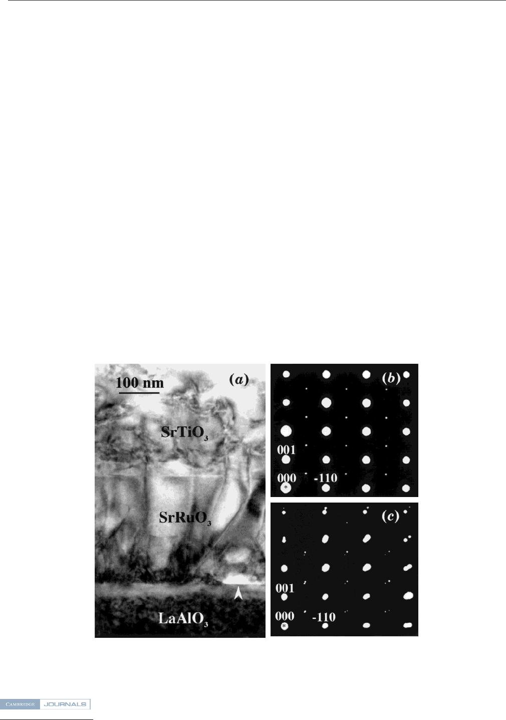
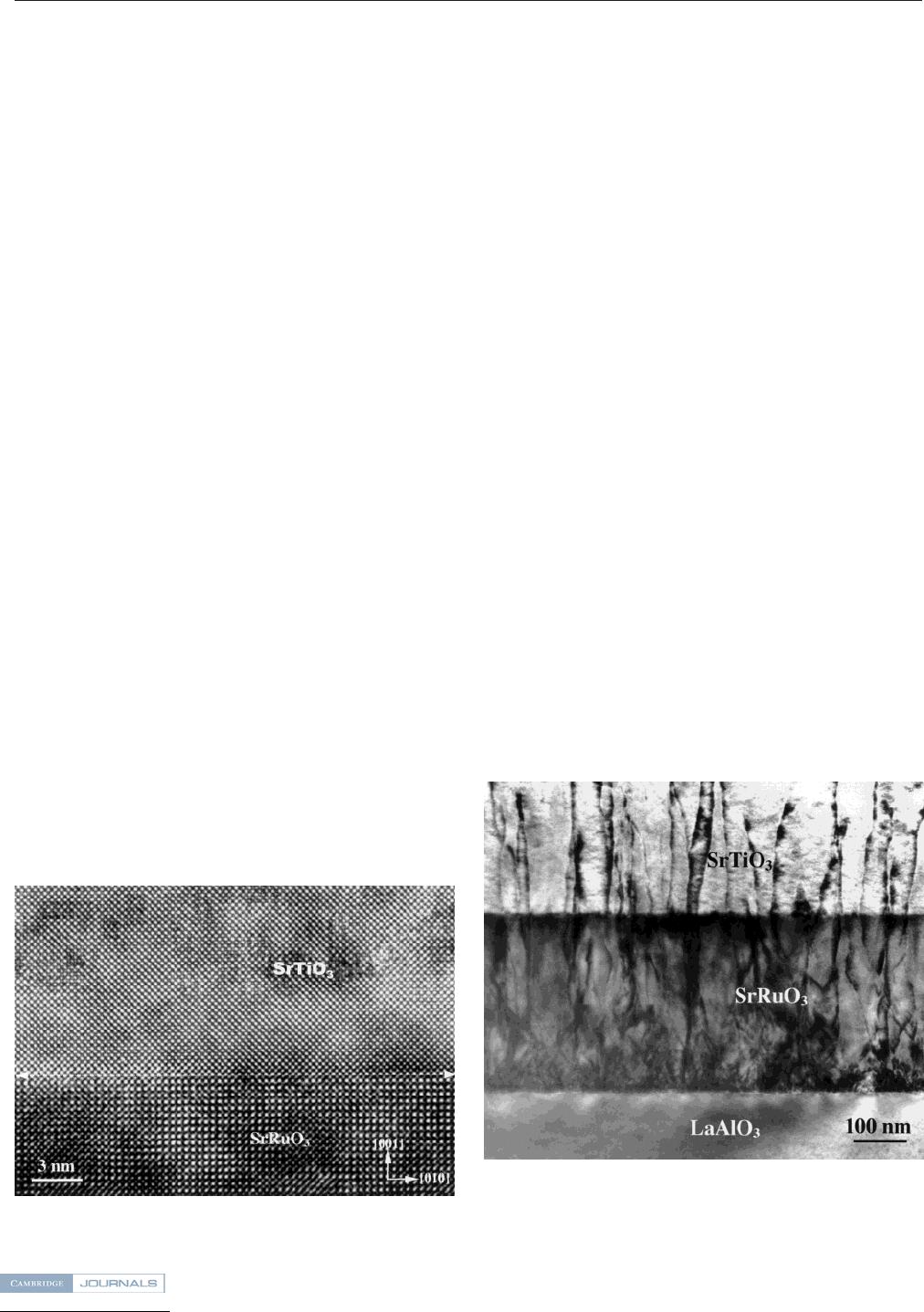
Figure 1(a) shows a low-magnification cross-sectional
image of a two-layer SrTiO
3
/SrRuO
3
film on LaAlO
3
taken along the [110] direction of the substrate. A high
density of defects can be observed along the SrRuO
3
/
LaAlO
3
interface. Some of the defects extend a signifi-
cant distance into the SrTiO
3
layer. Figure 1(b) is a
quarter of an electron diffraction pattern (EDP) obtained
by centering the selected-area diffraction aperture on the
SrTiO
3
/SrRuO
3
interface area. Figure 1(c) is the corre-
sponding pattern from the SrRuO
3
/LaAlO
3
interface
area. With reference to the pseudocubic cells of SrRuO
3
and LaAlO
3
, a simple cubic-to-cubic orientation relation-
ship can be derived from the EDP. The EDP of the
SrRuO
3
/LaAlO
3
interface area [Fig. 1(c)] consists of two
sets of diffraction spots which can easily be distin-
guished. The splitting of the spots indicates that a mis-
match relaxation between the SrRuO
3
and LaAlO
3
lattices has occurred. However, no splitting of the spots
can be detected in the pattern of the SrTiO
3
/SrRuO
3
in-
terface area [Fig. 1(b)].
To obtain information on the fine structure of the
defects at the SrRuO
3
/LaAlO
3
interface, we investi-
gated this interface along both the [100] and the [110]
FIG. 1. (a) Cross-sectional HRTEM image at low magnification of a SrTiO
3
/SrRuO
3
bilayer film on the LaAlO
3
substrate along the [110]
direction. An arrowhead shows a small hole at the SrRuO
3
/LaAlO
3
interface. A quarter of a superposed electron diffraction pattern taken (b) from
the SrTiO
3
/SrRuO
3
interface area and (c) from the SrRuO
3
/LaAlO
3
interface area, respectively. The central spots are indicated by an asterisk,
and the (
¯
110) and (001) diffraction spots are labeled in (b) and (c) by employing a notation for a pseudocubic structure.
J.S. Wu
et al.:
Microstructure and misfit relaxation in SrTiO
3
/SrRuO
3
bilayer films on LaAlO
3
(100) substrates
J. Mater. Res., Vol. 16, No. 12, Dec 20013444
http://journals.cambridge.org Downloaded: 11 Mar 2015 IP address: 203.64.11.45
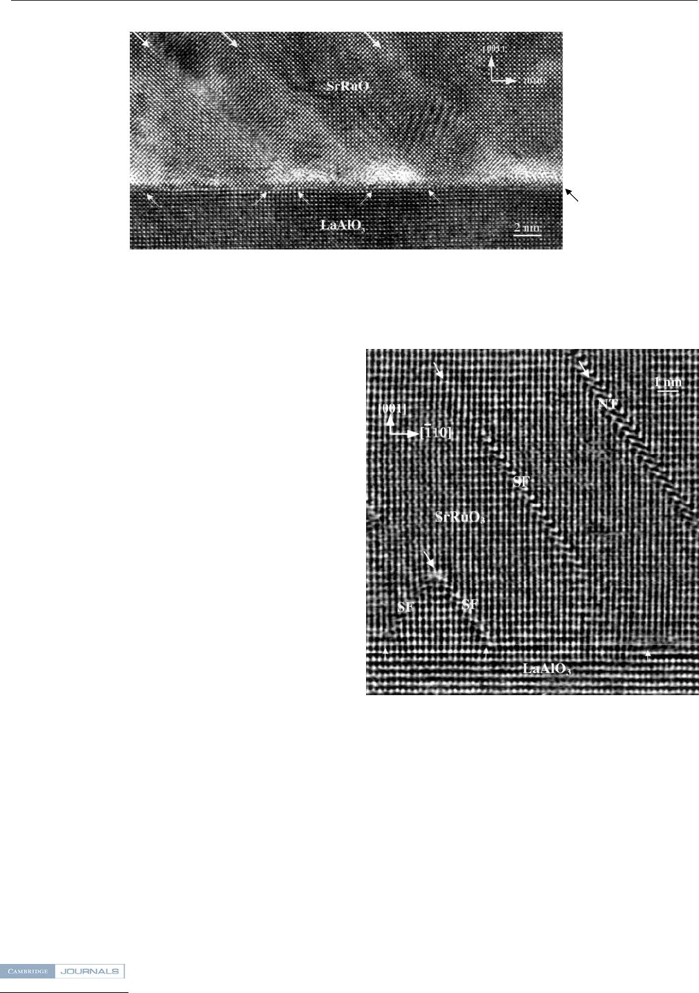
directions as shown in Figs. 2 and 3, respectively. If one
looks at the image in Fig. 2 along the 〈011〉 direction,
lattice planes in the LaAlO
3
substrate can be found to
terminate at the interface as indicated by small white
arrows. Associated with the termination of these lattice
planes, a change in image contrast appears in the SrRuO
3
layer both in the interface area and also farther away
from it, as shown by large white arrows. The change of
image contrast in Fig. 2 can be well understood by an
investigation of the interface area along the [110] direc-
tion as shown in Fig. 3. In this figure {111} planar de-
fects, stacking faults and nanotwins, can be seen as
indicated in the figure. Along the [110] direction, the
{111} defects are in edge on orientation so that they can
be identified easily. Every {111} planar defect is related
to one of the LaAlO
3
lattice planes terminating in the
interface as indicated by white arrows in the SrRuO
3
/
LaAlO
3
interface. In the left-hand part of Fig. 3, it is
interesting to note that the two stacking faults in the (1
¯
11)
and the (11
¯
1) plane, respectively, meet each other and are
pinned in the SrRuO
3
layer at about 4 nm above the
interface.
In the SrRuO
3
structure the stacking of atomic planes
along the 〈111〉 directions consists of alternating layers
of SrO
3
4−
and Ru
4+
.IfSrO
3
4−
layers are represented
by capital letters A, B, and C and the Ru
4+
layers by
lower-case letters a, b, and c, the stacking sequence in
the perfect crystal is AcBaCbAcBaCb. In studies of de-
fects in oxides, the stacking sequence of atomic planes
consisting of large ions can be used as a representation
to describe the defects in the crystals since small ions
are believed to move to their proper sites driven by
Coulomb force.
Nanotwins and stacking faults are two important
{111} planar defects in the perovskite structure. Two
basic types of faults, intrinsic and extrinsic, have to be
distinguished corresponding to the removal of a plane
from a perfect lattice or the insertion of an extra plane in
a perfect lattice, respectively. Such {111} faults can be
formed by propagation of partial dislocations. The glide
motion of Shockley partial dislocations with Burgers
vectors of the type 1/3〈112〉 can cause an intrinsic or an
extrinsic stacking fault in a BaTiO
3
crystal as described
by Eibl et al.
21
For example, the movement of a Shockley
partial dislocation transfers a {111} plane from the A to
FIG. 2. Cross-section HRTEM image of the interface between the SrRuO
3
layer and the LaAlO
3
substrate taken along the [100] direction, showing
a series of extra lattice planes terminating at the interface marked by small white arrows. The large white arrows denote a regular change of the
image contrast related to the termination of the extra planes.
FIG. 3. Cross-section HRTEM image of a SrRuO
3
/LaAlO
3
interface
taken along the [110] direction, showing three {111} stacking faults
(“SF”) and a nanotwin labeled “NT”. In the left part of the image, a
(1
¯
11) and a (11
¯
1) stacking fault terminate by their intersection.
J.S. Wu
et al.:
Microstructure and misfit relaxation in SrTiO
3
/SrRuO
3
bilayer films on LaAlO
3
(100) substrates
J. Mater. Res., Vol. 16, No. 12, Dec 2001 3445
http://journals.cambridge.org Downloaded: 11 Mar 2015 IP address: 203.64.11.45
B, B to C, and C to A position and thus changes the
stacking sequence from ABCABCAB to ABCBCABC
forming an intrinsic stacking fault. Stacking faults can
also form by the precipitation of point defects (vacancies
or interstitial atoms) in disk-shaped aggregates on the
{111} planes, i.e., by the climbing of Frank partial dis-
locations. It has been shown that {111} stacking faults
are formed by climb movement of a/3〈111〉 partial dis-
locations in BaTiO
3
thin films.
22
The formation of {111}
nanotwins can be understood as the result of stacking
faults extending in thickness.
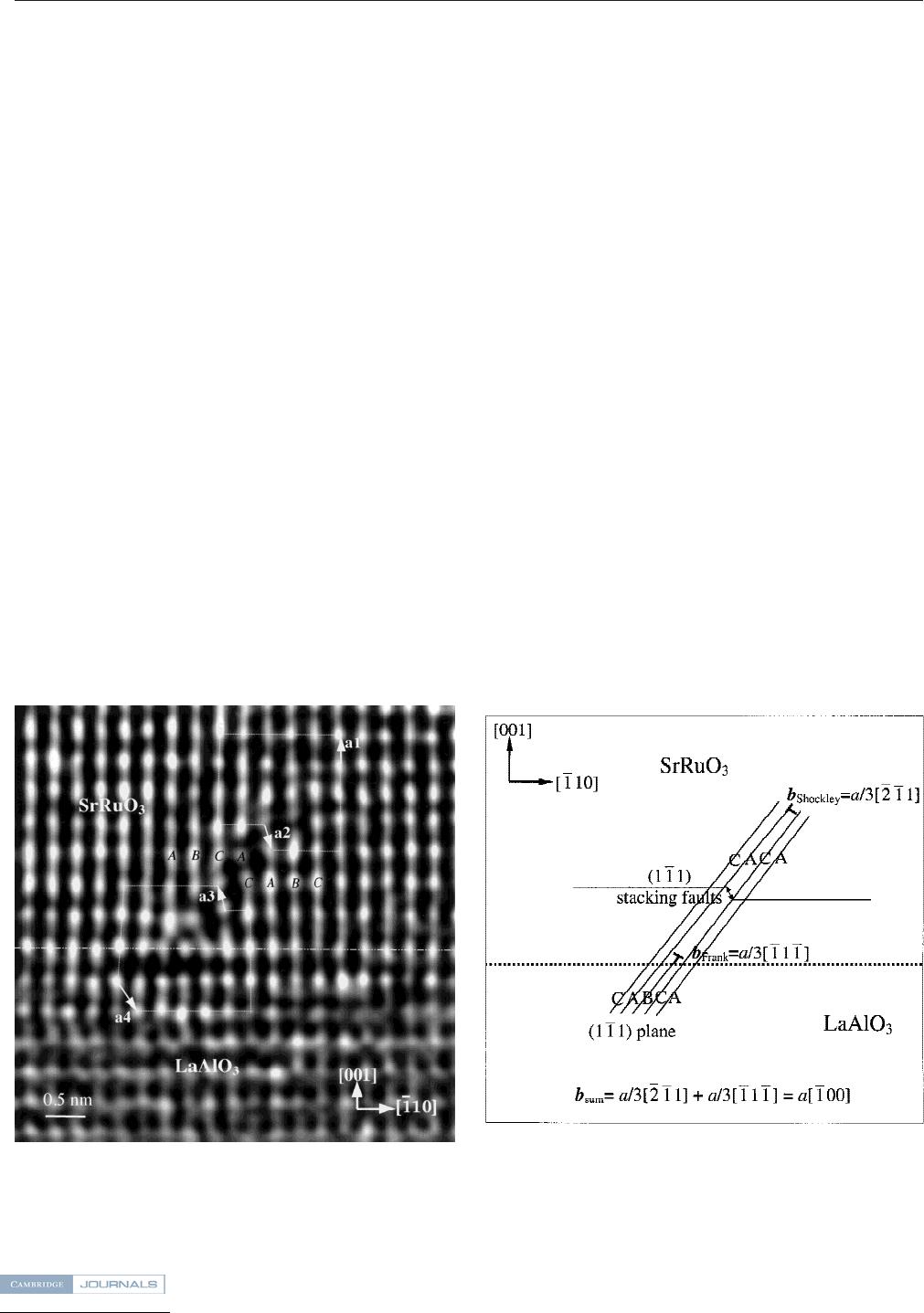
Figure 4 shows a stacking fault at the SrRuO
3
/LaAlO
3
interface. If the stacking notation introduced above is
employed, the stacking fault is identified as intrinsic type
with the ABCACABC sequence as indicated by the let-
ters. Burgers circuits are drawn to determine the dis-
placement vector at the ends of the stacking fault.
The projected displacement vector across the (11
¯
1)
stacking fault is a/6[1
¯
14
¯
] marked by the small white
arrow a2 (or a/6[11
¯
4] by arrow a3). At one end of the
stacking fault in the SrRuO
3
layer, the additional closure
failure is a[001] as indicated by the small white arrow a1.
The projected Burgers vector of the dislocation in the
SrRuO
3
layer thus can be determined as b
proj
⳱
a/6[1
¯
14
¯
]+a[001] ⳱ a/6[1
¯
12]. Unlike in the face-
centered cubic structure, a/6[1
¯
12] is not the Burgers
vector of the Shockley partial in the perovskite structure.
It is in fact the [110] projection of the Shockley partials
with the Burgers vector being either a/3[121] or
a/3[2
¯
1
¯
1]. At the other end in the substrate the additional
closure failure is a/2[1
¯
12
¯
] as indicated by the small white
arrow a4. With respect to the Burgers vector, the partial
dislocation at the end of the stacking fault at the inter-
face can therefore be characterized by b
proj
⳱ a/2[1
¯
12
¯
]+
a/6[11
¯
4] ⳱ a/3[1
¯
11
¯
]. This indicates a Frank partial dis-
location.
The geometrical configuration of the partials associ-
ated with the (11
¯
1) stacking fault in Fig. 4 is shown
in Fig. 5. The sum vector of the Shockley and the
Frank partial at both ends of the stacking fault is
b
sum
⳱ a[010] ⳱ a/3[1
¯
11
¯
]+a/3[121] or b
sum
⳱
a[1
¯
00] ⳱ a/3[1
¯
11
¯
]+a/3[2
¯
1
¯
1]. Therefore, the partials
and the accompanying stacking fault can be considered
as an extended dislocation dissociated from a perfect
dislocation with b ⳱ a〈100〉. Only one of the two pos-
sible cases is indicated in Fig. 5. Considering the value of
|b|
2
/a
2
as a measure for the dislocation energy, we obtain
1 ⳱ 3/9 + 6/9 before and after the reaction. Therefore,
the dissociation is not induced by self-energy but by
reduction of the strain energy in the interface area.
Obviously, the intrinsic stacking fault and its accom-
panying partial dislocation can contribute to the misfit
relaxation as that of perfect dislocation with Burgers
vector of a〈100〉. In fact, networks of the perfect mis-
fit dislocations with b ⳱ a〈100〉 have been observed
in perovskite films.
16,23
In this case, however, the
a〈100〉 type dislocation remains extended, like that in
the well-known system of a 30° partial and a 90° partial
FIG. 4. Image of a (11
¯
1) intrinsic stacking fault with stacking se-
quence ABCACABC at the SrRuO
3
/LaAlO
3
interface. Two Burgers
circuits are drawn to determine the Burgers vector of the dislocation
bounding the fault. The SrRuO
3
/LaAlO
3
interface is marked by a
dotted line.
FIG. 5. Geometric illustration of a partial dislocation pair bounding
the stacking fault in Fig. 4. The {111} planes are drawn as lines
and denoted by letters A, B, and C. The dotted line shows the
SrRuO
3
/LaAlO
3
interface, and the kink along the line parallel to [1
¯
10]
direction represents the intrinsic stacking fault. Two dislocations at the
ends of the stacking fault are indicated.
J.S. Wu
et al.:
Microstructure and misfit relaxation in SrTiO
3
/SrRuO
3
bilayer films on LaAlO
3
(100) substrates
J. Mater. Res., Vol. 16, No. 12, Dec 20013446
http://journals.cambridge.org Downloaded: 11 Mar 2015 IP address: 203.64.11.45
dissociated from a 60° misfit dislocation in the semi-
conducting films. The difference in the elastic moduli
of the LaAlO
3
crystal and the SrRuO
3
crystal can provide
the driving force for the dissociation of this dislocation
type. In this system the energy for maintaining a perfect
misfit dislocation in the interface can be higher than that
for two partials accompanying an intrinsic stacking fault.
Besides the {111} intrinsic stacking faults, extrinsic
stacking faults are also found in the SrRuO
3
/LaAlO
3
in-
terface. As shown in Fig. 6, an extrinsic stacking fault
can be identified referring to the stacking sequence of the
(1
¯
11) lattice planes which is ABCBABC as labeled. Em-
ploying a Burgers circuit consisting of two parts of clo-
sure failures as shown in the figure, we can identify the
dislocation at the end of the fault in the SrRuO
3
/LaAlO
3
interface. As shown by the arrows, a1 ⳱ a/3[11
¯
4
¯
]isthe
projected displacement vectors crossing the fault, while
a2 ⳱ a/2[1
¯
12
¯
] represents the additional closure failure.
The projected Burgers vector on the (110) plane of the
dislocation is thus b
proj
⳱ a/3[11
¯
4
¯
}+a/2[1
¯
12] ⳱
a/6[1
¯
12
¯
]. The Burgers vector of the dislocation can be
identified as either a/3[121
¯
]ora/3[2
¯
1
¯
1
¯
] as already dis-
cussed for Fig. 4.
The Shockley partial bounding the extrinsic stacking
fault in Fig. 6 at the SrRuO
3
/LaAlO
3
interface has edge
components of a/3〈120〉 in the interface plane, and the
extra lattice plane of the partial dislocation is on the side
of the LaAlO
3
substrate. Obviously, the extrinsic stack-
ing fault and its accompanying partial dislocation can
contribute to the misfit relaxation. Furthermore,
Wan et al.
24
showed that even for a null-type partial
dislocation dipole, which is formed by dissociation of a
screw threading dislocation, misfit strain could be re-
lieved, and the reduction of the misfit energy is propor-
tional to the width of the stacking fault.
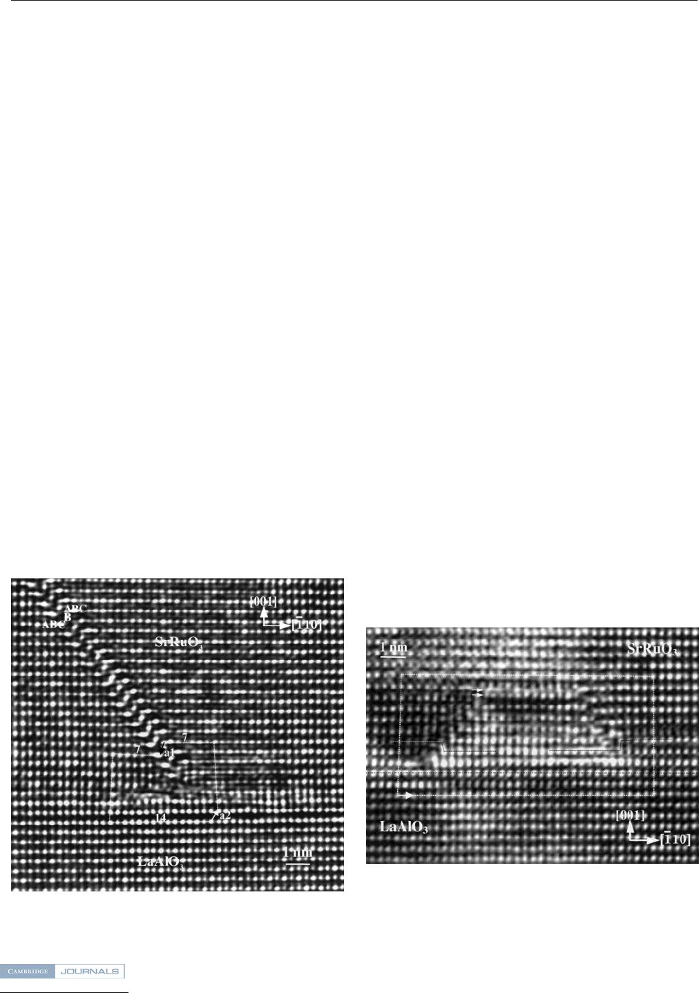
In addition to the introduction of isolated {111} planar
defects, the interaction of the defects also plays an im-
portant role in misfit accommodation. As shown in the
left-hand part of Fig. 3, two {111} intrinsic stacking
faults meet and interact with each other. At the end of the
two stacking faults in the interface, two Frank partial
dislocations can be identified, while at the meeting points
a stair-rod dislocation occurs.
25
The sum of the Burgers
vector of these three partials is a〈100〉. This implies
that the contribution of the two intrinsic stacking faults to
the misfit relaxation is equivalent to that of a perfect
〈100〉 misfit dislocation. This can be concluded by
performing a large Burgers circuit around the two stack-
ing faults.
Figure 7 shows a special configuration of two {111}
stacking faults and a (001) planar defect. It is a super-
dislocation from the dissociation of a 〈110〉 type dislo-
cation according to our previous identification.
26
The (001) defect denoted by two white arrows is a
Ruddlesden–Popper planar defect while the two stacking
faults indicated by dotted lines are identified as intrinsic
{111} faults. If a large Burgers circuit is employed
around the whole area, a closure failure with a displace-
ment vector a〈110〉 is obtained as shown in Fig. 7. This
implies that the configuration of a (001) planar defect and
of the two stacking faults induces about the same con-
tribution to the misfit relaxation as that of a perfect 〈110〉
type misfit dislocation. This shows that the {111} planar
defects and their interaction play an important role in
misfit accommodation in the SrRuO
3
/LaAlO
3
interface.
FIG. 6. Image of a (1
¯
11) extrinsic stacking fault with stacking se-
quence ABCBABC at the SrRuO
3
/LaAlO
3
interface. A Burgers circuit
is drawn to determine the dislocation bounding the fault.
FIG. 7. Image of a SrRuO
3
/LaAlO
3
interface taken along the [110]
direction showing two {111} intrinsic stacking faults and a (001)
planar defect. Two arrows show the (001) planar defect, while the
kinks in two black lines show the stacking faults. The SrRuO
3
/LaAlO
3
interface is marked by a dotted line.
J.S. Wu
et al.:
Microstructure and misfit relaxation in SrTiO
3
/SrRuO
3
bilayer films on LaAlO
3
(100) substrates
J. Mater. Res., Vol. 16, No. 12, Dec 2001 3447
http://journals.cambridge.org Downloaded: 11 Mar 2015 IP address: 203.64.11.45
On the basis of statistics investigations, we find that
the distribution of the {111} stacking faults along the
interface is inhomogeneous. Besides the partials con-
nected to {111} stacking faults, the system also employs
other means to reduce misfit strain. In fact, we observe
amorphous patches at the interface. In Fig. 1 there is a
small hole in the SrRuO
3
/LaAlO
3
interface as indicated
by an arrowhead. This is caused by a faster ion-milling
rate in an amorphous patch during sample preparation.
B. Misfit relaxation in the
SrTiO
3
/SrRuO
3
interface
Figure 8 shows an HRTEM image of the SrTiO
3
/
SrRuO
3
interface along the [100] direction. The perfect
interface is free of misfit dislocations as shown by a
dotted white line. In HRTEM images we usually ob-
served a layer with a thickness of about 5 nm directly
above the interface which shows brighter contrast than
other areas in the SrTiO
3
layer. Detailed investigation for
fully understanding of the contrast origin of the layer is
underway. According to the perovskite unit cells at the
room temperature, the SrRuO
3
has a larger parameter. If
we use the SrRuO
3
as a reference, the (010) planes spac-
ing of the SrTiO
3
will become a little bit larger so that it
can fit the value. If the volume of unit cell is considered
unchanged, however, the SrTiO
3
(001) planes spacing
should be a little bit shorter than its bulk value. In other
words, since the SrTiO
3
layer is in a tensile strain in the
(001) interface plane, the (100) and (010) lattice spacing
of the SrTiO
3
layer becomes larger and the (001) spac-
ing smaller in comparison with the bulk lattice param-
eter. Meanwhile, the similar analysis of lattice distortion
in SrRuO
3
layer can also be drawn consistent with the
fact that it is in a compressive strain. Thus, although
the crystal structure of the SrTiO
3
crystal should be cubic
structure at the room temperature it in fact has a little
tetragonal distortion in the film layer influenced by the
tensile strain due to the lattice misfit between the lattices
of SrTiO
3
and SrRuO
3
.
C. Structural defects in the SrTiO
3
layer
Figure 9 is a cross-section diffraction contrast image
of the bilayer film taken along a direction about 10° away
from the [110] zone axis. Near the SrRuO
3
/LaAlO
3
in-
terface, defects with high density occur to relax the lat-
tice misfit between the SrRuO
3
and the LaAlO
3
. The
density of the planar defects in the upper part of
the SrRuO
3
layer is lower due to the barrier effect of the
dislocations formed by interaction of the defects.
27
In
the SrTiO
3
layer most of the defects are related to ex-
tending stacking faults in the SrRuO
3
layer. We also
observed a kind of {110} antiphase boundary in the
SrTiO
3
layer introduced by an extrinsic stacking fault
arriving at the SrTiO
3
/SrRuO
3
interface. Details have
been discussed elsewhere.
28
Figure 10 shows two cross-section HRTEM images of
the SrTiO
3
/SrRuO
3
interface taken along the [110] di-
rection. While the SrTiO
3
/SrRuO
3
interface in (a) looks
quasi-continuous from top to bottom, double spot con-
trast can be seen in the interface in (b). Across the inter-
face in (a) the normal stacking sequence of perovskite
structure is preserved, while the interface in (b) shows
the structure of a Ruddlesden–Popper planar defect, as
schematically illustrated in (c) and (d).
Figure 11 shows a {110} planar defect starting at the
point where the two different types of interface meet
(white vertical arrow). The orientation of the interface on
FIG. 8. Cross-section image of a SrTiO
3
/SrRuO
3
interface taken along
the [100] direction.
FIG. 9. Cross-section image taken along the direction which is about
10° away from the [110] zone axis. Most of the defects in the SrTiO
3
layer are introduced from the defect propagating through the SrRuO
3
layer and reaching the SrTiO
3
/SrRuO
3
interface.
J.S. Wu
et al.:
Microstructure and misfit relaxation in SrTiO
3
/SrRuO
3
bilayer films on LaAlO
3
(100) substrates
J. Mater. Res., Vol. 16, No. 12, Dec 20013448
http://journals.cambridge.org Downloaded: 11 Mar 2015 IP address: 203.64.11.45
the left-hand side is slightly inclined to the viewing di-
rection so that the contrast is a little blurred.
However, the pairs of spots in the interface can still be
recognized. The interface in the right-hand part of the
image, however, exhibits a single spot contrast across
the interface. The {110} planar defect (note the faint
contrast line parallel to the vertical arrow) in the SrTiO
3
layer is produced by the conjunction of the two segments
of the SrTiO
3
/SrRuO
3
interface with different structure.
IV. CONCLUSIONS
In a study of the microstructure of the SrTiO
3
/SrRuO
3
two-layer films on the (100) LaAlO
3
substrates, we
found that the misfit between the SrRuO
3
layer and the
LaAlO
3
substrate is mainly accommodated by partial dis-
locations accompanying {111} planar defects in the area
of the SrRuO
3
/LaAlO
3
interface. Some defects propagate
through the SrRuO
3
layer and reach the SrTiO
3
/SrRuO
3
interface giving rise to defects in the SrTiO
3
layer. The
FIG. 11. HRTEM image along the [100] direction of a conjunction of
two types of SrRuO
3
/LaAlO
3
interface structure. A {110} planar de-
fect is generated at the conjunction.
FIG. 10. HRTEM images along the [110] direction showing two different SrTiO
3
/SrRuO
3
interface structures (a) and (b). The interface structures
are illustrated in (c) and (d).
J.S. Wu
et al.:
Microstructure and misfit relaxation in SrTiO
3
/SrRuO
3
bilayer films on LaAlO
3
(100) substrates
J. Mater. Res., Vol. 16, No. 12, Dec 2001 3449

http://journals.cambridge.org Downloaded: 11 Mar 2015 IP address: 203.64.11.45
misfit between the SrTiO
3
and the SrRuO
3
layers is,
however, mainly accommodated by elastic strain. Differ-
ent types of interface structure are found. In particular,
{110} planar defects in the SrTiO
3
layer are generated at
the interface area where a change of interface struc-
ture occurs.
ACKNOWLEDGMENTS
J.S.Wu is grateful for support from the Alexander von
Humboldt-Stiftung. The work at Pennsylvania State was
partially supported by NSF under Grant No. DMR-
9702632 and by the DARPA FAME Program under Con-
tract No. DABT63-98-1-002.
REFERENCES
1. C.B. Eom, R.J. Cava, R.M. Fleming, J.M. Philips, R.B. van Dover,
J.H. Marshall, J.W.P. Hsu, J.J. Krajewski, and W.F. Peck, Jr.,
Science 258, 1766 (1993).
2. X.D. Wu, S.R. Foltyn, R.C. Dye, Y. Coulter, and R.E. Muenchausen,
Appl. Phys. Lett. 62, 2434 (1993).
3. L. Antognazza, K. Char, T.H. Geballe, L.L.H. King, and
A.W. Sleight, Appl. Phys. Lett. 63, 1005 (1993).
4. R. Domel, C.L. Jia, C. Competti, G. Ockenfuss, and A.I. Branginski,
Supercond. Sci. Technol. 7, 277 (1994).
5. C.B. Eom, R.B. Van Dover, Julia M. Philips, D.J. Marshall,
C.H. Chen, R.J. Cava, R.M. Fleming, and D.K. Fork, Appl. Phys.
Lett. 63, 2570 (1993).
6. Q.X. Jia, X.D. Wu, S.R. Foltyn, and P. Tiwari, Appl. Phys. Lett.
66, 2197 (1995).
7. R.C. Neville, B. Hoeneisen, and C.A. Mead, J. Appl. Phys. 43,
2124 (1972).
8. O.G. Vendik, L.T. Ter-Martirosyanm, A.I. Dedyk, S.F. Karmanenko,
and R.A. Chakalov, Ferroelectrics 144, 33 (1993).
9. F. Selmi, R. Hughes, V.K. Varadan, and V.V. Varadan, Proc.
SPIE 1916, 180 (1993).
10. A.T. Findikoglu, C. Dought, S.M. Anlage, Qi Li, X.X. Xi, and
T. Venkatesan, J. Appl. Phys. 76, 2937 (1994).
11. C.H. Mueller, R.E. Treece, T.V. Rivkin, F.A. Miranda,
H.R. Moutinho, A. Swartzlander-Franz, M. Dalberth, and
C.T. Rogers, IEEE Trans. Appl. Supercond. 7, 3512 (1997).
12. H.C. Li, W.D. Si, A.D. West, and X.X. Xi, Appl. Phys. Lett. 73,
190 (1998).
13. J.W. Matthews, in Dislocations in Solids, edited by F.R.N. Nabarro
(North-Holland, Amsterdam, The Netherlands, 1979), Chap. 7.
14. A.F. Marshall, K. Char, R.W. Barton, A. Kapitulnik, and
S.S. Laderman, J. Mater. Res. 5, 2049 (1990).
15. W. Pompe, X. Gong, Z. Suo, and J.S. Speak, J. Appl. Phys. 74,
6012 (1993).
16. S. Stemmer, S.K. Streiffer, F. Ernst, and M. Ru¨hle, Phys. Status
Solidi A 147, 135 (1995).
17. T. Suzuki, Y. Nishi, and M. Fujimoto, Philos. Mag. A 79, 2461
(1999).
18. J.C. Jiang, W. Tian, X.Q. Pan, Q. Gan, and C.B. Eom, Appl. Phys.
Lett. 72, 909 (1998).
19. P. Lu, F. Chu, Q.X. Jia, and T.E. Mitchell, J. Mater. Res. 13, 2302
(1998).
20. R. Kilaas, Proc. 45th Annual EMSA meeting, Baltimore, MD,
edited by G.W. Bailey (San Francisco Press, San Francisco, CA
1987), p. 66.
21. O. Eibl, P. Pongratz, and P. Skalicky, Philos. Mag. B 57, 521
(1988).
22. C.L. Jia, K. Urban, M. Mertin, S. Hoffmann, and A. Waser,
Philos. Mag. A 77, 923 (1998).
23. T. Suzuki, Y. Nishi, and M. Fujimoto, Philos. Mag. A 79, 2461
(1999).
24. X.Y. Wan, J.W. Liang, M.L. Liu, and X.L. Jin, Phys. Rev. B 55,
9259 (1997).
25. J.S. Wu, C.L. Jia, K. Urban, J.H. Hao, and X.X. Xi, Philos. Mag.
Lett. 81, 375 (2001).
26. J.S. Wu, C.L. Jia, K. Urban, J.H. Hao, and X.X. Xi, J. Cryst.
Growth, in press.
27. J.S. Wu, C.L. Jia, K. Urban, J.H. Hao, and X.X. Xi, Philos.
Mag. A (in press).
28. J.S. Wu, C.L. Jia, K. Urban, J.H. Hao, and X.X. Xi, J. Appl. Phys.
89, 5653 (2001).
J.S. Wu
et al.:
Microstructure and misfit relaxation in SrTiO
3
/SrRuO
3
bilayer films on LaAlO
3
(100) substrates
J. Mater. Res., Vol. 16, No. 12, Dec 20013450
